
Formation method of interconnect structure

A technology of interconnect structure and orthosilicate, which is applied in the direction of electrical components, semiconductor/solid-state device manufacturing, circuits, etc., can solve the problems that cannot meet the development requirements of semiconductor technology, poor performance of conductive plugs, etc., and achieve good flatness, Effects of improving filling performance and increasing consumption rate

Active Publication Date: 2018-08-10
SEMICON MFG INT (SHANGHAI) CORP
View PDF3 Cites 0 Cited by
  • Summary
  • Abstract
  • Description
  • Claims
  • Application Information

AI Technical Summary

Problems solved by technology

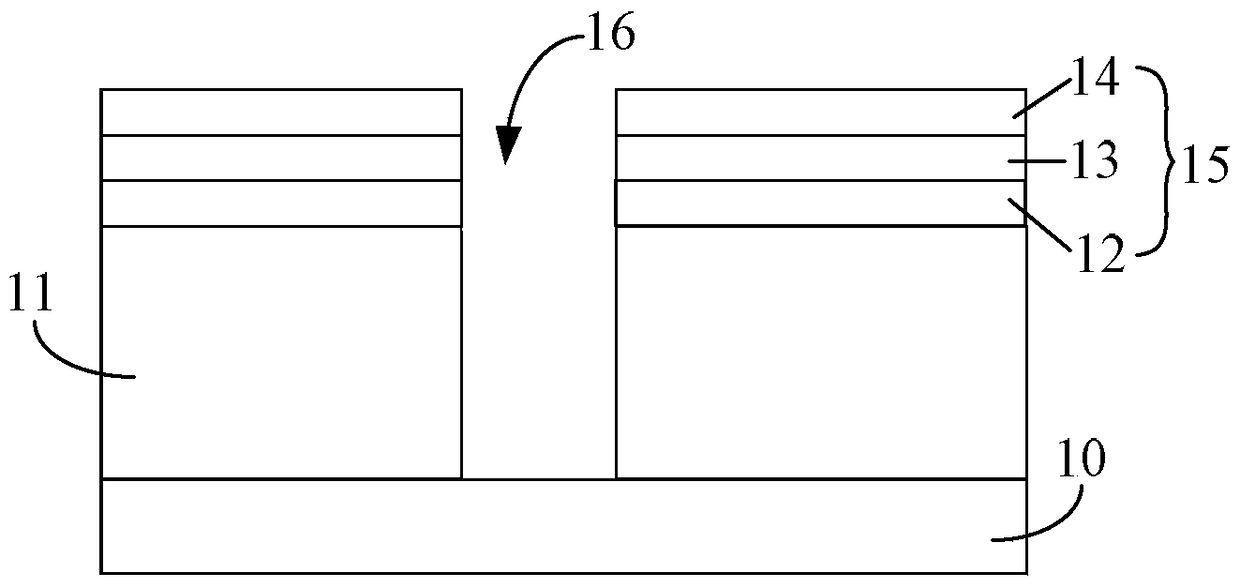
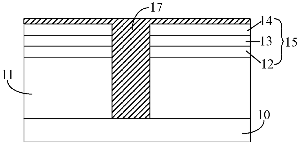
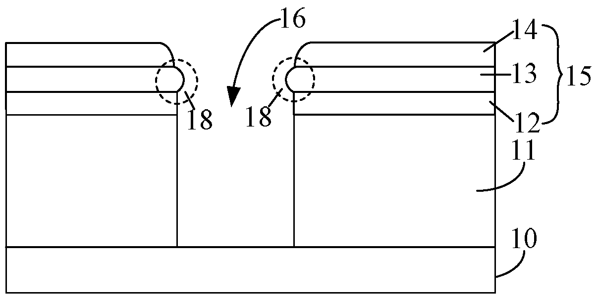
[0007] However, in the actual operation process, it is found that the performance of the conductive plug formed by the existing technology is poor and cannot meet the development requirements of semiconductor technology. Therefore, how to improve the performance of the conductive plug is an urgent problem to be solved by those skilled in the art.

Method used


Image

  • Formation method of interconnect structure
  • Formation method of interconnect structure
  • Formation method of interconnect structure

Examples


Embodiment 1

[0048] Figure 4 ~ Figure 15 It is a structural schematic diagram of an embodiment of the method for forming the interconnection structure of the present invention.

[0049] The forming method of the interconnection structure provided in this embodiment includes:

[0050] first reference Figure 4 As shown, a substrate 20 is provided.

[0051] In this embodiment, the base 20 includes: a semiconductor substrate. Alternatively, the base 20 includes a semiconductor substrate and semiconductor components formed in the semiconductor substrate or on the surface of the semiconductor substrate.

[0052] The semiconductor substrate is a silicon substrate, a silicon germanium substrate, a silicon carbide substrate, a silicon-on-insulator (SOI) substrate, a germanium-on-insulator (GOI) substrate, a glass substrate or other III-V compound substrates , The semiconductor substrate material does not limit the protection scope of the present invention.

[0053] A first insulating layer 2...

Embodiment 2

[0100] join Figure 16 and 17 , is a structural schematic diagram illustrating another embodiment of the method for forming the interconnection structure of the present invention.

[0101] The method for forming the interconnection structure of this embodiment and Figure 4 to Figure 15 The similarities of the illustrated embodiments will not be repeated, and the differences are:

[0102] In this embodiment, the silicon oxide mask layer formed on the low-K dielectric mask layer 24 has a single-layer structure, and the forming steps include:

[0103] refer to Figure 16 , first forming a tetraethylorthosilicate layer 361 on the low-K dielectric material layer 24, and then performing an oxygen plasma treatment on the tetraethylorthosilicate layer 361, so that the oxygen plasma and the The tetraethylorthosilicate layer 361 is reacted to form a silicon oxide mask layer 362 .

[0104] In order to reduce the carbon atoms in the silicon oxide mask layer 362, the flow rate of oxy...


PUM


Abstract

The invention provides a formation method for an interconnecting structure. The formation method comprises the steps of forming a dielectric layer on a semiconductor substrate; and then forming a silicon oxide masking layer on the dielectric layer for forming a hard mask, wherein the step of forming the silicon oxide masking layer is carried out by the steps of forming a tetraethyl orthosilicate layer on the dielectric layer firstly; then performing oxygen plasma processing on the tetraethyl orthosilicate layer to enable the oxygen plasma to react with the tetraethyl orthosilicate layer to form the silicon oxide masking layer. The carbon content in the silicon oxide layer formed by the technology is obviously reduced, so that the shortcoming that the consume rate of the silicon oxide masking layer is obviously less than that of the dielectric layer caused by the carbon atoms in a cleaning process for the through holes by a wet method after the through holes are formed by the subsequent dielectric layer is overcame, the flatness of the overall side wall of the openings formed in the hard mask and the through holes in the dielectric layer is effectively improved, therefore, the filling performance of the conductive materials subsequently filled to the through holes is improved, and the performance of a formed conductive plug is further improved.

Description

technical field [0001] The invention relates to the technical field of semiconductors, in particular to a method for forming an interconnection structure. Background technique [0002] With the development of semiconductor technology, the integration level of semiconductor devices continues to increase, and the feature size (Critical Dimension, CD) of semiconductor devices becomes smaller and smaller. [0003] With the gradual reduction of the feature size of the semiconductor device, the RC delay (RC delay) problem of the interconnection structure has more and more influence on the semiconductor device. Reducing the K value of the dielectric layer material in the interconnection structure is an effective method to reduce the RC delay effect. In recent years, in the Back End of The Line (BEOL) of semiconductor devices, low K dielectric constant (Low K, LK) materials (K<3) and ultra-low K dielectric constant (Ultra Low K , ULK) material has gradually become the mainstrea...

Claims


Application Information

Patent Timeline
Patent Type & Authority Patents(China)
IPC IPC(8): H01L21/768
Inventor 周鸣
Owner SEMICON MFG INT (SHANGHAI) CORP
Learn More