Wafer cutting method possessing test pattern
A cutting method and a technology for testing patterns, which are used in manufacturing tools, fine working devices, electrical components, etc., can solve the problems of chip damage, delamination, chip cracking stress, etc., to reduce the occupied area, improve cutting efficiency, improve The effect of the cut effect
- Summary
- Abstract
- Description
- Claims
- Application Information
AI Technical Summary
Problems solved by technology
Method used
Image

Examples
Embodiment 1
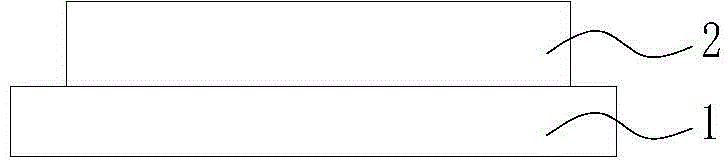
[0041] Firstly, a wafer to be cut is provided, and 4a shows a partial schematic view of the wafer to be cut, including a plurality of spaced apart chip regions 100 (4 chip regions in the figure), and scribes are arranged between each chip region 100 The scribe groove area 102 , the scribe groove area 102 includes a cutting area 104 and a test component 101 . Wherein, the test assembly 101 is a copper interconnected test structure circuit and an online monitoring pattern, and its main material is copper; and an insulating material layer is provided on the lower surface of the test assembly 101, preferably, the insulating material layer is a silicon nitride film , in order to avoid the downward diffusion of copper and cause damage to the device.
[0042] In this embodiment, the cutting area 104 and the test assembly 101 do not form an overlap, so that when cutting along the cutting area 104, the test assembly 101 will not form contact with the copper interconnection, thereby avo...
Embodiment 2
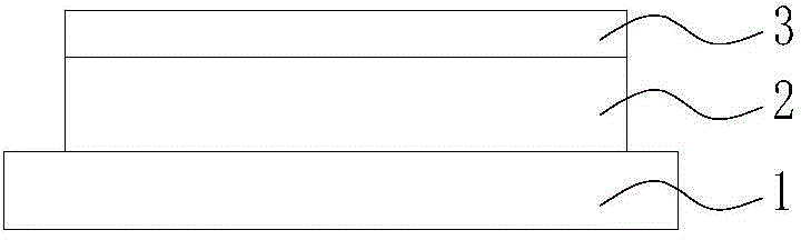
[0044] Firstly, a wafer to be cut is provided, and 5a is a partial schematic diagram of the wafer to be cut, including a plurality of chip regions 100 spaced apart, and scribe groove regions 102 are arranged between adjacent chip regions 100 . Each chip area 100 is provided with a test assembly 101 at the corner away from the scribe groove area 102. The test assembly 101 is a copper interconnected test structure circuit and an online monitoring pattern. Its material is copper, and it is arranged on the lower surface of the test assembly 101. There is a layer of insulating material, preferably, the insulating material layer is a silicon nitride film, so as to avoid the downward diffusion of copper and damage to the device.
[0045] Since the test assembly 101 in the present invention is not arranged in the scribe groove area 102, the entire scribe groove area 102 can be directly cut as the cutting area, so the width of the scribe groove area 102 can be appropriately reduced, and...
PUM
| Property | Measurement | Unit |
|---|---|---|
| Width | aaaaa | aaaaa |
Abstract
Description
Claims
Application Information
 - Generate Ideas
- Intellectual Property
- Life Sciences
- Materials
- Tech Scout
- Unparalleled Data Quality
- Higher Quality Content
- 60% Fewer Hallucinations
Browse by: Latest US Patents, China's latest patents, Technical Efficacy Thesaurus, Application Domain, Technology Topic, Popular Technical Reports.
© 2025 PatSnap. All rights reserved.Legal|Privacy policy|Modern Slavery Act Transparency Statement|Sitemap|About US| Contact US: help@patsnap.com