Manufacturing method of low temperature polysilicon thin film transistor

A thin-film transistor and low-temperature polysilicon technology, which is used in semiconductor devices, electrical components, circuits, etc., can solve the problems of increased heat generation of TFT devices, adverse product reliability, etc., and achieves favorable heat dissipation, small channel size, and electrical stability. Effect

Active Publication Date: 2018-07-17
WUHAN CHINA STAR OPTOELECTRONICS TECH CO LTD
View PDF3 Cites 0 Cited by
  • Summary
  • Abstract
  • Description
  • Claims
  • Application Information

AI Technical Summary

Problems solved by technology

However, while the electron mobility of LTPS is improved, the heat generation of TFT devices is also increased, which is not conducive to the reliability of products.

Method used


Image

  • Manufacturing method of low temperature polysilicon thin film transistor
  • Manufacturing method of low temperature polysilicon thin film transistor
  • Manufacturing method of low temperature polysilicon thin film transistor

Examples


Embodiment Construction

[0024] The present invention will be described in detail below in conjunction with the accompanying drawings and embodiments.

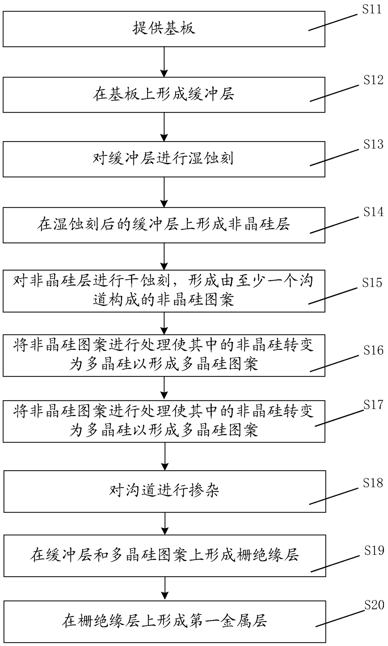
[0025] see figure 1 , figure 1 It is a flow chart of a preferred embodiment of the manufacturing method of the low-temperature polysilicon thin film transistor of the present invention. In this embodiment, the manufacturing method of the low-temperature polysilicon thin film transistor includes the following steps:

[0026] Step S11: providing a substrate.

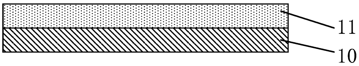
[0027] In step S11, please combine figure 1 refer to figure 2 , figure 2 It is a schematic diagram of the substrate and the first buffer layer in steps S11 and S12 of the manufacturing method of the low-temperature polysilicon thin film transistor of the present invention. Providing the substrate 10 may specifically provide a glass substrate, or providing the substrate 10 may specifically provide a ceramic substrate, or providing the substrate 10 may specifically provide a quartz substrate...


PUM

PropertyMeasurementUnit
thicknessaaaaaaaaaa
thicknessaaaaaaaaaa

Abstract

The present invention discloses a method for manufacturing a low-temperature polysilicon thin film transistor. The method comprises the steps of providing a substrate, forming a buffer layer on the substrate, carrying out wet etching on the buffer layer, forming an amorphous silicon layer on the buffer layer which is subjected to wet etching, carrying out drying etching on the amorphous silicon layer to form an amorphous silicon pattern formed by at least one channel, partly etching the buffer layer, processing the amorphous silicon pattern such that amorphous silicon in the amorphous silicon pattern is converted into polysilicon to form a polysilicon pattern, doping the channel, forming a gate insulation layer on the buffer layer and the polysilicon pattern, and forming a first metal layer on the gate insulation layer. Through the above mode, the channel width value of the low-temperature polysilicon thin film transistor can be obviously reduced, the line distance between thin film transistors is increased, and the heat radiation of the low-temperature polysilicon thin film transistor is facilitated.

Description

technical field [0001] The invention relates to the technical field of liquid crystal display, in particular to a method for manufacturing a low-temperature polysilicon thin film transistor. Background technique [0002] LTPS (Low Temperature Poly-Silicon, low temperature polysilicon) display screens have been widely used in small-sized products, and many mainstream mobile phones in the market currently use LTPS display screens. LTPS technology can form a high-mobility polysilicon semiconductor layer on a glass substrate by laser annealing and other methods, so that the display screen has the advantages of high resolution, high aperture ratio, high response speed, and low power consumption. However, while the electron mobility of LTPS is improved, the calorific value of the TFT device is also increased, which is not conducive to the reliability of the product. [0003] Therefore, it is necessary to provide a method for manufacturing a low-temperature polysilicon thin film t...

Claims


Application Information

Patent Timeline
Patent Type & Authority Patents(China)
IPC IPC(8): H01L29/10H01L29/66
CPCH01L29/1033H01L29/66757
Inventor 孟林
Owner WUHAN CHINA STAR OPTOELECTRONICS TECH CO LTD
Why Eureka
Try Eureka