

A kind of three-dimensional memory and its preparation method
A memory, three-dimensional technology, applied in electrical components and other directions, can solve the problem of low space utilization of gating switches, and achieve the effects of reducing leakage current and thermal crosstalk, simplifying process steps, and reducing cell surface.
- Summary
- Abstract
- Description
- Claims
- Application Information
AI Technical Summary
Problems solved by technology
Method used
Image


Examples
preparation example Construction
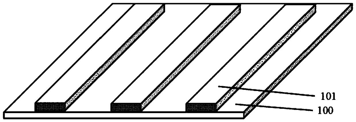
[0071] Please refer to Figures 1-15. The present invention also provides a method for preparing a multi-layer three-dimensional memory, which is described by taking a double-layer memory as an example. The method includes:
[0072] Step 1: Carry out photolithography on the insulating or semiconductor substrate 100, and then prepare a layer of lower electrode 101 in the vertical direction on the substrate 100 after photolithography, and peel off to obtain the lower electrode 101 corresponding to the photolithographic pattern. The electrode material can be metal or non-metal with good conductivity, such as silver, copper, titanium-tungsten alloy, graphene, etc. The thickness of the lower electrode 101 is 100-500nm, and the structure after step 1 is shown in Figure 1;
[0073] Step 2: prepare another layer of lower electrothermal insulation layer 102, the material of the lower electrothermal insulation layer 102 is: nitride, oxide, sulfide or a mixture of two or more materials, th...
Embodiment 1
[0086] Step 1: Carry out photolithography on the silicon substrate with a layer of silicon dioxide insulating layer on the surface, and then prepare a layer of lower electrode on the substrate after photolithography. After peeling off, a strip-shaped lower electrode in the vertical direction is obtained. The electrode thickness is 100nm, and the lower electrode material is silver;
[0087] Step 2: Prepare another layer of lower electrothermal insulating layer, the lower insulating layer is slightly smaller than the lower electrode on the substrate, so that the lower electrode is partially exposed, the thickness is 500nm, and the material is SiO 2 ;
[0088] Step 3: Use micro-nano processing technology to prepare small holes in the middle of the lower electrothermal insulation layer, with a diameter of 50nm and a depth of 500nm;
[0089] Step 4: using chemical vapor deposition to fill the lower n-type semiconductor material plug column, the thickness of the n-type semiconducto...
Embodiment 2
[0100] Step 1: Carry out photolithography on the silicon substrate with a layer of silicon dioxide insulating layer on the surface, and then prepare a layer of lower electrode on the substrate after photolithography. After peeling off, a strip-shaped lower electrode in the vertical direction is obtained. The electrode thickness is 100nm, and the bottom electrode material is titanium;
[0101] Step 2: Prepare another layer of lower electrothermal insulating layer, the lower insulating layer is slightly smaller than the lower electrode on the substrate, so that the lower electrode is partially exposed, the thickness is 500nm, and the material is SiO 2 ;
[0102] Step 3: Use micro-nano processing technology to prepare small holes in the middle of the lower electrothermal insulation layer, with a diameter of 50nm and a depth of 500nm;
[0103] Step 4: using chemical vapor deposition to fill the lower n-type semiconductor material plug column, the thickness of the n-type semicondu...
PUM
| Property | Measurement | Unit |
|---|---|---|
| thickness | aaaaa | aaaaa |
| diameter | aaaaa | aaaaa |
| thickness | aaaaa | aaaaa |
Abstract
Description
Claims
Application Information