Femtosecond laser-controlled silicon surface nanopillar preparation method based on dual-wavelength electronic dynamic control

An electronic dynamic control, femtosecond laser technology, applied in the field of femtosecond laser applications, can solve the problem of high requirements for base materials, and achieve the effect of improving processing accuracy and processing efficiency

Active Publication Date: 2016-04-20
BEIJING INSTITUTE OF TECHNOLOGYGY
View PDF7 Cites 33 Cited by
  • Summary
  • Abstract
  • Description
  • Claims
  • Application Information

AI Technical Summary

Problems solved by technology

[0003] The purpose of the present invention is to solve the problem that the existing processing technology of crystalline silicon nanocolumns has high requirements on substrate materials, and to provide a method for preparing nanocolumns on the silic...

Method used


Image

  • Femtosecond laser-controlled silicon surface nanopillar preparation method based on dual-wavelength electronic dynamic control

Examples


Embodiment 1

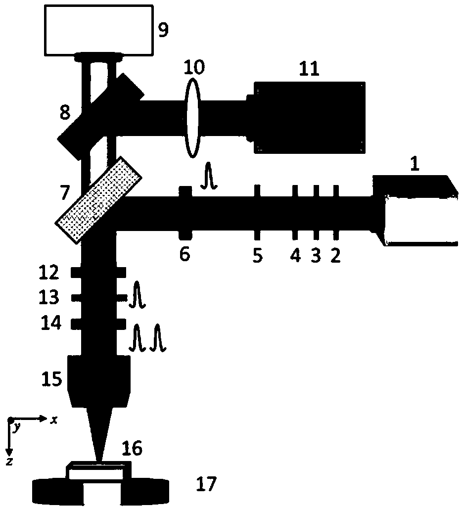
[0029] Taking the processing of single crystal silicon nanopillar arrays as an example, using the dual-wavelength femtosecond excitation processing method of the present invention, the dual-wavelength fundamental frequency and double-frequency pulses used are both linearly polarized, and the specific processing steps are as follows:

[0030] Adjust the optical path to ensure that the incident direction of the laser is perpendicular to the surface of the processed sample;

[0031](1) Sample preparation: In this example, a 20nm gold film was coated on a 10mm×10mm×1mm monocrystalline silicon sample by vacuum sputtering (the thickness of the gold film can be adjusted from 10nm to 40nm); Limited to the method of vacuum sputtering, thermal evaporation or any other method that can coat the metal film on the sample to be processed can also be used; the metal can be any metal that can be excited to generate plasmonic polaritons under the action of laser pulses , preferably gold or silv...

Embodiment 2

[0039] Taking the processing of single crystal silicon nanopillar arrays as an example, using the dual-wavelength femtosecond laser processing method of the present invention, the dual-wavelength fundamental-frequency optical pulses used are circularly polarized, and the double-frequency optical pulses are linearly polarized. The specific processing steps are as follows :

[0040] Other steps are identical with embodiment 1, and difference is: do not pass through the basic frequency light polarization direction adjustment process of step (4), add quarter-wave plate 13 before frequency doubling crystal 14, adjust quarter-wave plate 13. Make the angle between the optical axis direction of the wave plate and the original laser polarization direction 45° to obtain circularly polarized 800nm ​​femtosecond laser pulses. The processing is carried out under the condition that the fundamental frequency light is circularly polarized.

Embodiment 1、2

[0041] Embodiment 1, 2 comparative results:

[0042] Since the SPPs field of the PL-like structure under the excitation of the second circularly polarized laser is uniformly distributed along the radial direction of the structure, the stress generated by the extrusion of the material toward the center is more uniform, so in Example 2, two pulses of circularly polarized fundamental frequency light are used for processing The nano-column structure on the surface of the crystalline silicon is not easy to bend, and the shape is better.


PUM

PropertyMeasurementUnit
Thicknessaaaaaaaaaa
Thicknessaaaaaaaaaa

Abstract

The invention relates to a femtosecond laser-controlled silicon surface nanopillar preparation method based on dual-wavelength electronic dynamic control, and belongs to the technical field of femtosecond laser application. The method comprises the steps that on the basis of local instant electronic exciting dynamic control, the wave length of the fundamental frequency laser is converted into 400 nm from 800 nm through a frequency doubling technology, and the surface micro-nano structural morphology is controlled by adopting a dual-wavelength femtosecond laser, wherein a first beam generates a generic plasma lens structure (PL) on the surface of a material, a second beam generates surface plasma along the edge of the generic PL structure and generates a gradient field distributed along the center of a light spot, and then the material generates the force extruding towards the center under the action of the pulse to form a convex nanopillar structure; preparation of large-area uniform nanopillar arrays is achieved through control over a procedure of a processing platform. Compared with an existing method, the preparation method has the advantages that the nanopillar processing precision and processing efficiency are effectively improved, efficient and precise control over the crystalline silicon surface nano structure is achieved, and the application value on the aspects such as information storage and solar cells is achieved.

Description

technical field [0001] The invention relates to a method for preparing nano-columns on the surface of crystal silicon controlled by a femtosecond laser based on dual-wavelength electronic dynamic control, and belongs to the technical field of femtosecond laser applications. Background technique [0002] The surface micro-nanostructure of solid materials is an important factor to control the optical, wettability, chemical, biological and other characteristics of the material surface. Therefore, effective adjustment and control of the micro-nanostructure of the solid material surface has become a research focus. With the emergence of mode-locking and amplification technology, femtosecond laser technology has developed rapidly. Femtosecond laser surface micro-nano processing has become a novel and effective surface treatment technology, which can process different forms of micro-nano structures on solid surfaces, and is widely used in optoelectronics, biosensing, micro-nano flu...

Claims


Application Information

Patent Timeline
IPC IPC(8): B23K26/06B23K26/08B23K26/352
CPCB23K26/06B23K26/067
Inventor 姜澜韩伟娜李晓炜
Owner BEIJING INSTITUTE OF TECHNOLOGYGY
Why Eureka
Try Eureka