Formation method of transistor

A transistor and dry etching technology, which is applied in semiconductor devices, semiconductor/solid-state device manufacturing, electrical components, etc., can solve the problems that the electrical properties of transistors need to be improved, and the transistor formation process is difficult to control, so as to achieve good appearance and improve electrical properties. performance effect

Active Publication Date: 2016-04-20
SEMICON MFG INT (SHANGHAI) CORP
View PDF4 Cites 5 Cited by
  • Summary
  • Abstract
  • Description
  • Claims
  • Application Information

AI Technical Summary

Problems solved by technology

[0004] Although the introduction of a high-k metal gate can reduce the leakage current of the transistor to a certain extent, the electrical performance of the transistor formed by the prior art still needs to be improved due to the difficulty in controlling the formation process of the transistor.

Method used


Image

  • Formation method of transistor
  • Formation method of transistor
  • Formation method of transistor

Examples


Embodiment Construction

[0036] It can be known from the background art that the performance of the transistor formed in the prior art needs to be improved.

[0037] Research is conducted on the formation method of the transistor. In one embodiment, taking the transistor to be formed as a CMOS transistor as an example, the formation method of the transistor includes the following steps:

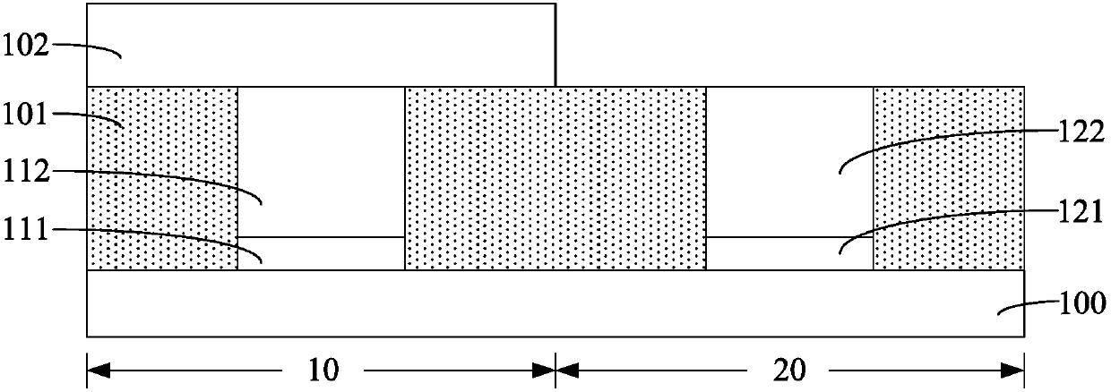
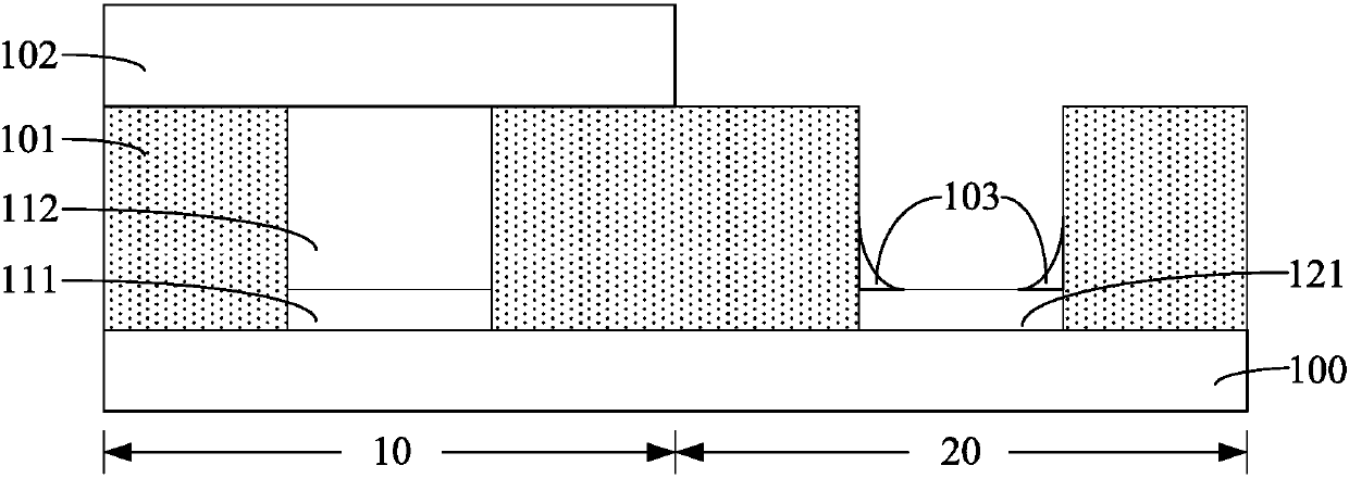
[0038] Such as figure 1 As shown, a substrate 100 is provided. The substrate 100 includes a first region 10 and a second region 20. A first dummy gate structure is formed on the surface of the substrate 100 in the first region 10. The first dummy gate structure includes: A gate dielectric layer 111 and a first dummy gate 112 located on the surface of the first gate dielectric layer 111, a second dummy gate structure is formed on the surface of the substrate 100 in the second region 20, and the second dummy gate structure includes: a second A gate dielectric layer 121 and a second dummy gate 122 located on the surface...


PUM


Abstract

The invention provides a formation method of a transistor. The formation method of a transistor comprises providing a substrate, wherein a pseudo-grid is arranged on the substrate; forming an interlayer dielectric layer covered on the surface of the substrate and the surface of the side wall of the pseudo-grid, wherein the top of the interlayer dielectric layer flushes with the surface of the top of the pseudo-grid; forming a mask layer on the surface of the interlayer dielectric layer, wherein the mask layer exposes the surface of the top of the pseudo-grid; taking the mask layer to remove the pseudo-grid for mask layer etching, and forming a groove in the interlayer dielectric layer wherein a root defect is formed on the surface of the side wall of the bottom of the groove; and utilizing a dry etching process to remove the root defect. The formation method of a transistor utilizes the dry etching process to remove the root defect after removing the pseudo-grid so as to improve the morphology, of the grid, formed in the groove subsequently and optimize the electrical performance of a formed transistor.

Description

technical field [0001] The invention relates to the technology in the field of semiconductor manufacturing, in particular to a method for forming a transistor. Background technique [0002] The main semiconductor device of an integrated circuit, especially a very large scale integrated circuit, is a metal-oxide-semiconductor field effect transistor (MOS transistor). With the continuous development of integrated circuit manufacturing technology, the technology node of semiconductor devices is continuously reduced, and the geometric size of transistors is continuously reduced following Moore's law. When the size of the transistor is reduced to a certain extent, various secondary effects caused by the physical limit of the transistor appear one after another, and it becomes more and more difficult to scale down the feature size of the transistor. Among them, in the field of transistor and semiconductor manufacturing, the most challenging thing is how to solve the problem of la...

Claims


Application Information

Patent Timeline
Patent Type & Authority Applications(China)
IPC IPC(8): H01L21/336
CPCH01L21/823437H01L21/823828H01L29/66636H01L29/7848H01L29/165H01L21/32137H01L29/66545H01L29/517H01L29/495H01L29/4966H01L29/401
Inventor 张海洋张璇
Owner SEMICON MFG INT (SHANGHAI) CORP
Why Eureka
Try Eureka