Organic Photosensitive Devices with Exciton-Blocking Charge Carrier Filtering Layers
An electronic device and organic technology, applied in the field of organic photosensitive optoelectronic devices, can solve problems such as hindering device performance
- Summary
- Abstract
- Description
- Claims
- Application Information
AI Technical Summary
Problems solved by technology
Method used
Image

Examples
Embodiment 1
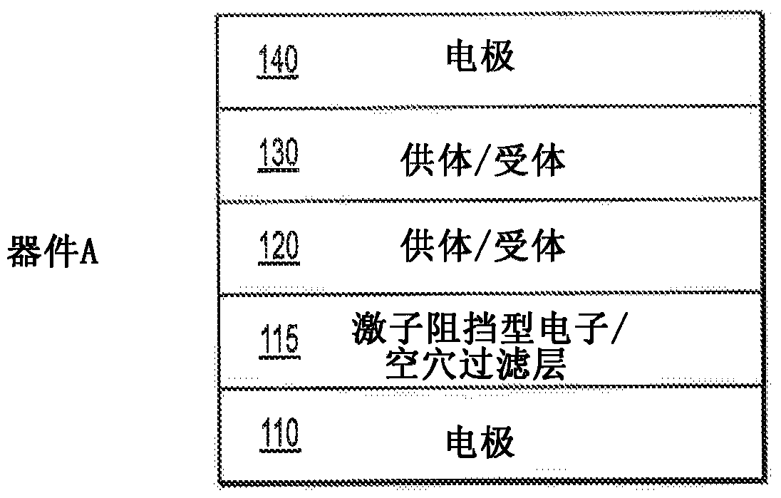
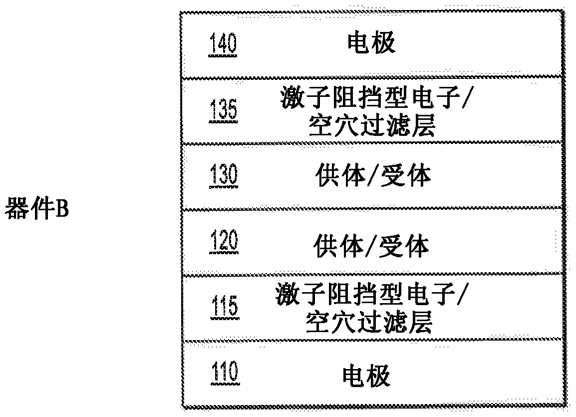
[0153] C 60 Mix with bathocuproine (BCP) at various concentrations to form an exciton blocking electron filter layer. BCP is a wide energy gap material with ratio C 60 (singlet 1.86eV, triplet 1.55eV) high singlet (3.17eV) and triplet (2.62eV) energies and LUMO (-1.6eV), making BCP an inert dopant and preventing 60 Both energy and electron transfer. The doped C 60 : BCP films effectively block excitons while still conducting electrons. Based on these properties, the doped film acts as a buffer / filter layer, resulting in improved device performance compared to devices with other buffer layers.
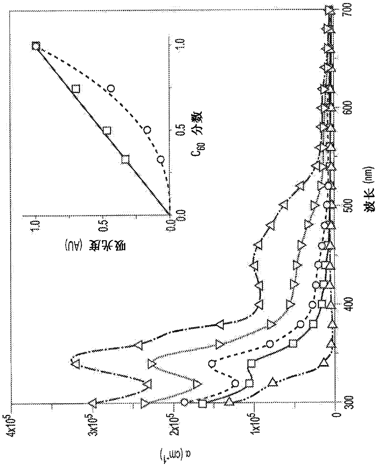
[0154] Effect of BCP doping on fullerene absorption by making various volume ratios of C 60 : BCP film for research. figure 2 shows pure and doped C 60 The absorption spectrum of the film. When C 60 As the fraction decreases, the absorption weakens and approaches that of BCP. However, if figure 2 Depicted in the inset of , the decays of the two absorption peaks at 340 nm an...
Embodiment 2
[0156] The device was fabricated as follows: a glass substrate coated with patterned ITO (patterned stripe width 2mm, thickness=150±10nm; sheet resistance=20±5Ωcm-2; transmittance 84% at 550nm; courtesy of Thin Film Devices, Inc.) Clean with soap and boil in perchloroethylene, acetone and propanol (5 min each). The ITO substrate was exposed to an ozone atmosphere (UVOCS T10X10 / OES) for 10 min, and then immediately loaded into a high vacuum chamber. The deposition rate of a pure material layer is as follows: MoO x (0.02nm / s), NPD (0.1nm / s), C 60 (0.1nm / s), BCP (0.1nm / s) and Al (0.2nm / s). doped film (C 60 : BCP content by volume) deposition rate is as follows: C 60 :BCP(2:1) – codeposited C 60 (0.08nm / s): BCP (0.04nm / s); C 60 :BCP(1:1) – codeposited C 60 (0.06nm / s): BCP (0.06nm / s); C 60 :BCP(1:2) – codeposited C 60 (0.04nm / s): BCP (0.08nm / s). After organic deposition, place a mask with a stripe width of 2 mm on the N 2 down on the substrate and deposit a 100 nm Al cat...
Embodiment 3
[0164] Figure 4 The device shown in was fabricated according to the fabrication method disclosed in Example 2. Figure 4 The J-V curves of the device and the external quantum efficiency curves as a function of wavelength under one solar AM1.5G illumination are shown, and the device structure is in the inset. (x = 10 nm (D7), 20 nm (D6), and 30 nm (D5)). Table 2 provides performance data for this device.
[0165] Table 2: Device Performance Data
[0166]
PUM
 Abstract
Description
Claims
Application Information
 - R&D
- Intellectual Property
- Life Sciences
- Materials
- Tech Scout
- Unparalleled Data Quality
- Higher Quality Content
- 60% Fewer Hallucinations
Browse by: Latest US Patents, China's latest patents, Technical Efficacy Thesaurus, Application Domain, Technology Topic, Popular Technical Reports.
© 2025 PatSnap. All rights reserved.Legal|Privacy policy|Modern Slavery Act Transparency Statement|Sitemap|About US| Contact US: help@patsnap.com