Deposition method of crystalline silicon battery back electrode, and obtained crystalline silicon battery

A crystalline silicon cell and deposition method technology, applied in the solar field, can solve problems such as increasing the fragmentation rate, and achieve the effects of reducing absorption, increasing current, and eliminating depressions and voids

Active Publication Date: 2016-05-11
CSI CELLS CO LTD
View PDF3 Cites 6 Cited by
  • Summary
  • Abstract
  • Description
  • Claims
  • Application Information

AI Technical Summary

Problems solved by technology

[0006] If the thickness of the silicon wafer continues to be thinned below 100μm, a depth of about 20μm of the depression (silicon of the substrate is consumed) may see a more obvious effect on the current reduction. In addition, the cavity formed by the depression that is not filled with co-gold may be It will also increase the fragmentation rate, so it is necessary to reduce the depth of the depression at the local contact of the PERC battery and reduce the void at the same time

Method used


Image

  • Deposition method of crystalline silicon battery back electrode, and obtained crystalline silicon battery
  • Deposition method of crystalline silicon battery back electrode, and obtained crystalline silicon battery
  • Deposition method of crystalline silicon battery back electrode, and obtained crystalline silicon battery

Examples


specific Embodiment approach 1

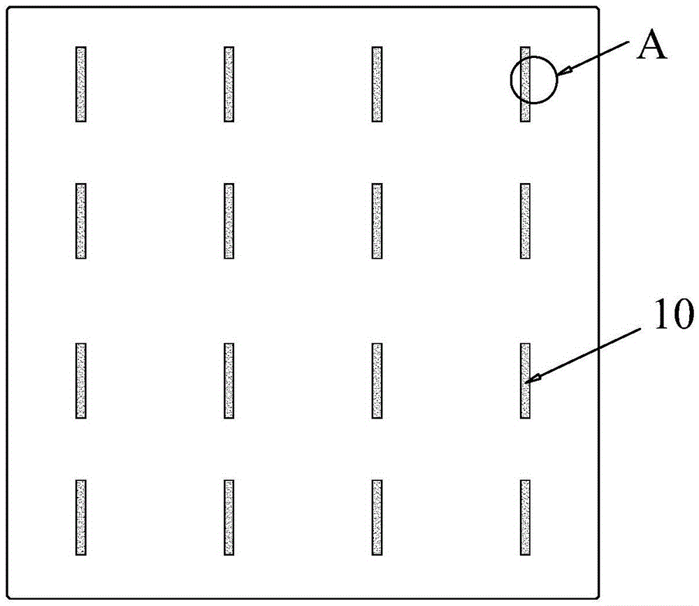
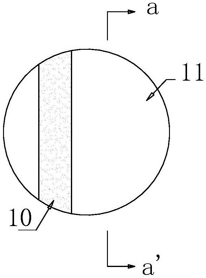
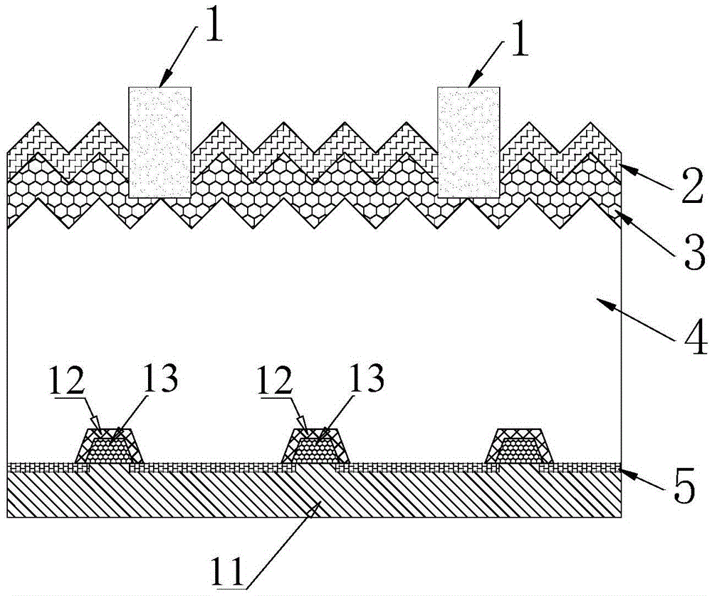
[0093] The specific embodiment one provides a PERC battery, the specific structure is as follows Figure 4~6 as shown ( Figure 4 The front view of the PERC battery structure schematic diagram provided for Embodiment 1, Figure 5 A partially enlarged front view of part A of the structural schematic diagram of the PERC battery provided for Embodiment 1, Image 6 Part A of the structural schematic diagram of the PERC battery provided for specific embodiment 1 along b-b' side view), includes the following structure:

[0094]The p-type silicon chip 4, the textured n+ doped layer 3 and the textured passivation film 2 arranged on the front side of the p-type silicon chip 4 in sequence, and the textured Ag electrode arranged on the textured passivation film 2 1;

[0095] There is a first passivation film 5 on the back side of the p-type silicon wafer 4, and there are a plurality of openings on the first passivation film 5; the inside of the openings is filled with electrodes 8 con...

Embodiment 1

[0097] Embodiment 1 provides the first preparation process of the PERC battery back structure obtained in Embodiment 1, which specifically includes the following steps:

[0098] (1) On the back side of the p-type silicon chip 4 with the partial opening of the passivation film distributed according to requirements, the back silver electrode 10 is deposited by screen printing;

[0099] (2) Printing and depositing an electrode 8 containing aluminum element at the partial opening, and the electrode 8 containing aluminum element is Ruxing Technology RX8201;

[0100] (3) screen printing silver paste on the back of the p-type silicon wafer 4 to obtain a barrier layer 7, the barrier layer 7 covers the electrode 8 containing aluminum;

[0101] (4) Continue to deposit a conductive electrode 9 on the back of the p-type silicon wafer 4, the conductive electrode 9 is Ruxing Technology 28D9, and the conductive electrode 9 covers the passivation of the barrier layer 7 and the back of the p-t...

Embodiment 2

[0105] Example 2 provides the second preparation process of the back structure of the PERC cell obtained in Embodiment 1, which specifically includes the following steps:

[0106] (1) Screen-print an electrode 8 at the partial opening on the back of the p-type silicon wafer 4 with the partial opening of the passivation film, and the electrode 8 is Ruxing Technology RX8256;

[0107] (2) Deposit a silver electrode on the back of the p-type silicon wafer 4, the deposition range is the predetermined position of the back silver electrode 10 to form the back silver electrode 10, and the local opening covers the electrode 8 containing aluminum element to form a barrier Layer 7, the barrier layer 7 is silver paste, and the deposition method is screen printing;

[0108] (4) Continue to deposit the conductive electrode 9 on the back of the p-type silicon wafer 4 , the conductive electrode 9 covers the barrier layer 7 and the passivation film area on the back of the p-type silicon wafer ...


PUM

PropertyMeasurementUnit
widthaaaaaaaaaa
thicknessaaaaaaaaaa
depthaaaaaaaaaa

Abstract

The invention relates to a deposition method of a crystalline silicon battery back electrode. The method is characterized in that an electrode capable of preventing dissolving diffusion of element silicon to element aluminum at a preset temperature is deposited around the periphery of the local opening of crystalline silicon undergoing a passive film local opening technology; or the electrode capable of preventing dissolving diffusion of element silicon to element aluminum at the preset temperature is deposited around the periphery of the predetermined local opening position of crystalline silicon undergoing a passive film generation technology; and the preset temperature is not greater than 950DEG C. The method can eliminate recesses and cavities in the local contact position in current common aluminum silicon sintering processes, and reduces absorption of a sintered aluminum layer to long-wavelength photons; and local back field, local electric contact and mechanical tension are formed through arranging an electrode, so the back reflection of a PERC battery is further improved, and the current is improved.

Description

technical field [0001] The present invention relates to the field of solar cell preparation, in particular to a deposition method for the back electrode of a crystalline silicon cell and the obtained crystalline silicon cell, in particular to a PERC cell or an N-type back junction cell with local aluminum doping to form a p+ layer and form a contact The deposition method of the back electrode, and the obtained PERC battery or an N-type back junction battery with local aluminum doping to form a p+ layer and form a contact. Background technique [0002] Solar photovoltaic power generation is an important part of new energy, and the core technology of photovoltaic power generation is crystalline silicon cell technology. Passivated Emitter and Back Local Contact Cell (PERC) was first researched by the University of New South Wales. Because the battery is passivated on both sides, the back electrode adopts the form of local contact, which effectively reduces the surface recombina...

Claims


Application Information

Patent Timeline
Patent Type & Authority Applications(China)
IPC IPC(8): H01L31/0224H01L31/068
CPCH01L31/022425H01L31/068Y02E10/547
Inventor 张高洁吴坚王栩生邢国强
Owner CSI CELLS CO LTD
Why Eureka
Try Eureka