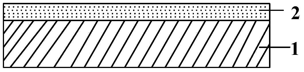
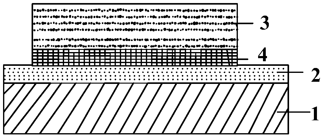
A method for bonding compound semiconductors and silicon-based semiconductors
A semiconductor and compound technology, applied in semiconductor/solid-state device manufacturing, electrical components, circuits, etc., can solve the problems of poor bonding effect, less than ideal, and high bonding temperature, and achieve thin dielectric, easy integration, and low bonding temperature. Effect
- Summary
- Abstract
- Description
- Claims
- Application Information
AI Technical Summary
Problems solved by technology
Method used
Image

Examples
Embodiment Construction
[0027] This embodiment provides a method for bonding a compound semiconductor indium phosphide and a silicon wafer, including the following steps:
[0028] (1) Prepare a 4-inch (100) crystal-oriented circular silicon wafer and perform standard RCA cleaning. The specific steps are as follows
[0029] A) Cleaning solution I, solution II and solution III used for RCA cleaning are configured; solution I is ammonia water (mass concentration 27%): hydrogen peroxide (mass concentration 30%): deionized water=1:1:5 volume ratio configuration; solution II It is configured as hydrofluoric acid (mass concentration 50%): deionized water = 1:50 volume ratio; solution III is hydrochloric acid (mass concentration 37%): hydrogen peroxide (mass concentration 30%): deionized water = 1:1:6 Volume ratio configuration.
[0030] B) Clean the silicon wafers in turn as follows: soak in solution I for 10 minutes at 80°C, put in deionized water for 1 minute, then soak the silicon wafers in solution II,...
PUM
 Abstract
Description
Claims
Application Information