Semiconductor device and manufacturing method therefor

A technology for semiconductors and devices, applied in the field of semiconductor devices and their preparation, can solve the problems of increasing parasitic gate-source capacitance and parasitic resistance, increasing parasitic gate-source capacitance and parasitic resistance, and increasing on-resistance, etc. Breakdown voltage, reduce parasitic gate-source capacitance and parasitic resistance, reduce leakage effect

Active Publication Date: 2016-06-01
DYNAX SEMICON
View PDF4 Cites 10 Cited by
  • Summary
  • Abstract
  • Description
  • Claims
  • Application Information

AI Technical Summary

Problems solved by technology

[0004] However, in the above-mentioned semiconductor device, the source field plate 111 directly covers the second dielectric layer 110, and the metal of the source field plate 111 with a large area completely overlaps with the gate 108 below it and the two-dimensional electron gas in the channel, resulting in a parasitic gate The source capacitance, the parasitic gate-source capacitance is inversely proportional to the distance between the source field plate 111 and the gate 108, and is proportional to the overlapping area between the source field plate 111 and the gate 108, and the dielectric constant of the dielectric layer is relatively large, Therefore, a large parasitic gate-source capacitance Cgs will be generated during the operation of the device, resulting in the deterioration of the frequency characteristics of the device, and because the source field plate 111 is generally connected to the lowest potential, it will affect the distribution of the two-dimensional electron gas below it, making the two-dimensional electron gas Expanding into the channel layer reduces the concentration of two-dimensional electron gas in the channel, thereby generating parasitic resistance, which makes the on-resistance increase during the working process of the device
And affected by the thickness of the dielectric layer, the source field plate 111 is far away from the strong electric field area, and the modulation effect on the strong electric field is limited. Thinning the thickness of the dielectric layer can improve the electric field modulation effect of the source field plate 111, but the parasitic gate-source capacitance and parasitic resistance It will increase, and thickening the thickness of the dielectric layer can reduce the parasitic gate-source capacitance and parasitic resistance, but it will furth

Method used


Image

  • Semiconductor device and manufacturing method therefor
  • Semiconductor device and manufacturing method therefor
  • Semiconductor device and manufacturing method therefor

Examples


Embodiment 1

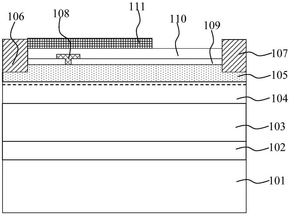
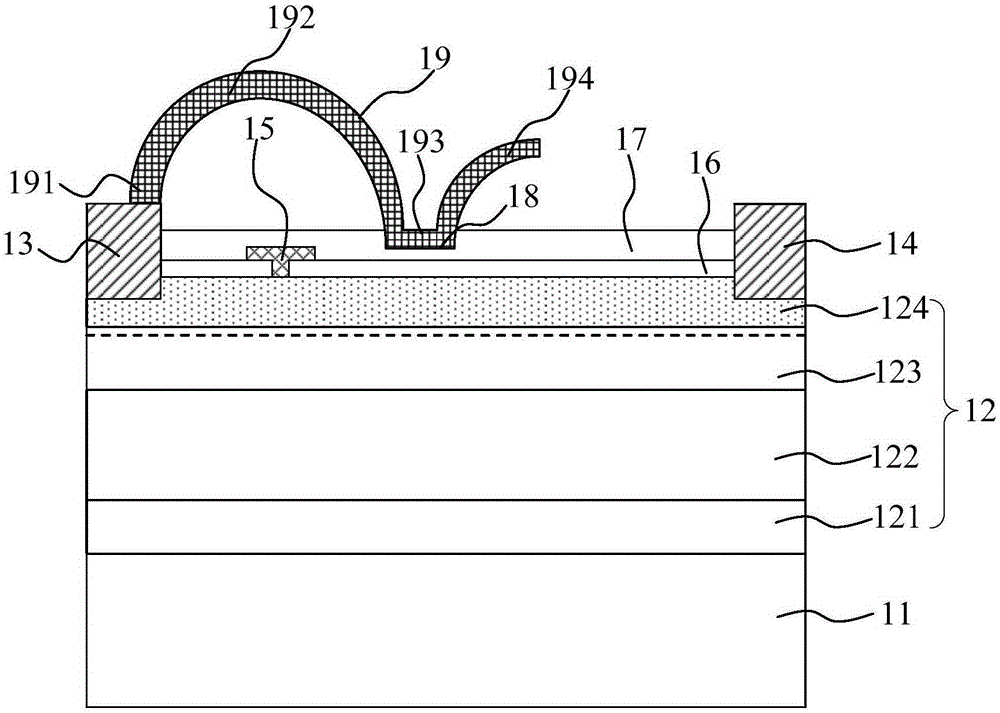
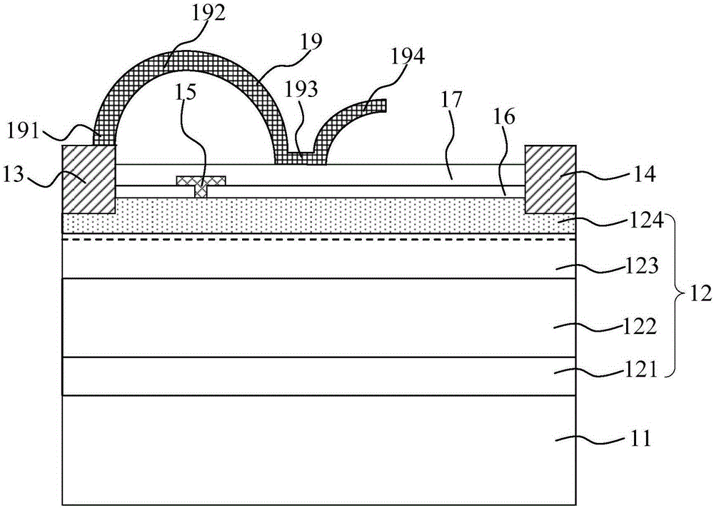
[0033] Figure 2a-Figure 2c is a schematic cross-sectional view of a semiconductor device with a dielectric layer provided in Embodiment 1 of the present invention, image 3 It is a top view of the semiconductor device provided by Embodiment 1 of the present invention. Such as Figure 2a-Figure 2c As shown, the semiconductor device includes a substrate 11; a semiconductor layer 12 on the substrate 11; a source 13 on the semiconductor layer 12, a drain 14, and a gate 15 between the source 13 and the drain 14; The source field plate 19 located on the semiconductor layer 12 includes in turn an initial portion 191 electrically connected to the source level 13, a first intermediate portion 192 with air between the semiconductor layer 12, and covering between the gate 15 and the drain 14. The second middle portion 193 on the semiconductor layer 12 and the tail portion 194 where air exists between the semiconductor layer 12 . Wherein, the material of the source field plate 19 is a...

Embodiment 2

[0071] Figure 6 It is a schematic cross-sectional view of a semiconductor device with a sloped groove wall provided in Embodiment 2 of the present invention. This embodiment is optimized on the basis of the above-mentioned embodiments, as shown in Figure 6 As shown, the semiconductor device may include: a substrate 11; a semiconductor layer 12 on the substrate 11; a source 13 on the semiconductor layer 12, a drain 14, and a gate between the source 13 and the drain 14 15; the first dielectric layer 16 and the second dielectric layer 17 on the semiconductor layer 12; the groove 18 on the second dielectric layer 17 between the grid 15 and the drain 14, the groove 18 passes through the air bridge light Formed by a self-aligned etching process; the source field plate 19 located on the second dielectric layer 17, the initial portion 191 of the source field plate 19 is electrically connected to the source 13, and the first middle portion 192 of the source field plate 19 is connecte...

Embodiment 3

[0080] Figure 8 A schematic cross-sectional view of a semiconductor device in which the dielectric layer is one layer provided for Embodiment 3 of the present invention, as shown in Figure 8 As shown, this embodiment is based on the above-mentioned embodiments, and the second dielectric layer 17 is removed, which is equivalent to the gate region, the region between the gate and the source, and the second part of the region between the gate and the drain. Dielectric layer 17 is replaced by air of equal thickness, can further reduce parasitic capacitance and parasitic resistance like this, groove 18 is etched on the first dielectric layer 16 simultaneously, covers the second middle part 193 distances in groove 18 The closer the electric field area, the more effective the modulation of the electric field between the gate and the drain is.


PUM

PropertyMeasurementUnit
Lengthaaaaaaaaaa

Abstract

The invention provides a semiconductor device and a manufacturing method therefor. The device comprises a substrate, a semiconductor layer positioned on the substrate, a source electrode and a drain electrode positioned on the semiconductor layer, and a grid electrode positioned between the source electrode and the drain electrode, and a source field plate positioned on the semiconductor layer, wherein a groove is formed in the semiconductor layer between the grid electrode and the drain electrode; and the source field plate comprises a beginning part electrically connected with the source electrode, a first middle part, a second middle part covering the semiconductor layer between the grid electrode and the drain electrode, and a tail part, wherein air exists between the first middle part and the semiconductor layer, and between the tail part and the semiconductor layer. According to the semiconductor device, the overlay deviation between the groove and the source field plate can be eliminated, so that the production cost can be saved, and parasitic gate source capacitance and parasitic resistance are reduced as well.

Description

technical field [0001] The invention relates to the technical field of semiconductors, in particular to a semiconductor device and a preparation method thereof. Background technique [0002] HEMT (High Electron Mobility Transistor, High Electron Mobility Transistor) device working under high drain-source voltage, the electric field lines near the side of the gate near the drain end are very dense, which will form a high electric field peak, and the high electric field in this local area can It causes a very large gate leakage current, even leads to material breakdown, and the device fails, thereby reducing the breakdown voltage of the device, and the higher the electric field peak, the smaller the breakdown voltage that the device can withstand. At the same time, with the increase of time, the high electric field will also cause the degradation and denaturation of the dielectric layer or semiconductor material layer on the surface of the device, which will affect the reliabi...

Claims


Application Information

Patent Timeline
IPC IPC(8): H01L29/778H01L21/335H01L29/40
CPCH01L29/402H01L29/66431H01L29/778H01L29/7786H01L29/2003H01L29/407
Inventor 张乃千刘飞航金鑫裴轶宋晰
Owner DYNAX SEMICON
Why Eureka
Try Eureka