AlN template, preparation method of AlN template and semiconductor device on AlN template

A semiconductor and nitride semiconductor technology, applied in semiconductor devices, electrical components, circuits, etc., can solve the problems of poor wavelength uniformity of epitaxial wafers, large warpage of epitaxial wafers, and large compressive stress of GaN epitaxy, and achieve improved wavelength uniformity, Good crystal quality, the effect of increasing the lattice constant

Active Publication Date: 2016-06-01
HC SEMITEK SUZHOU
View PDF9 Cites 11 Cited by
  • Summary
  • Abstract
  • Description
  • Claims
  • Application Information

AI Technical Summary

Problems solved by technology

[0005] In order to solve the problems that when GaN epitaxy is grown on the existing AlN template, the compressive stress in the GaN epitaxy is too large, the epitaxial wafer has a large warp, and the wavelength uniformity of the epitaxial wafer is poor, the embodiment of the present invention provides a A kind of AlN template, the preparation method of AlN template and the semiconductor device on AlN template

Method used


Image

  • AlN template, preparation method of AlN template and semiconductor device on AlN template
  • AlN template, preparation method of AlN template and semiconductor device on AlN template
  • AlN template, preparation method of AlN template and semiconductor device on AlN template

Examples


Embodiment Construction

[0032] In order to make the object, technical solution and advantages of the present invention clearer, the implementation manner of the present invention will be further described in detail below in conjunction with the accompanying drawings.

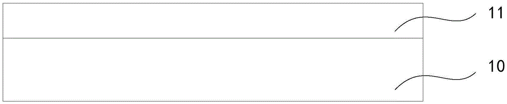
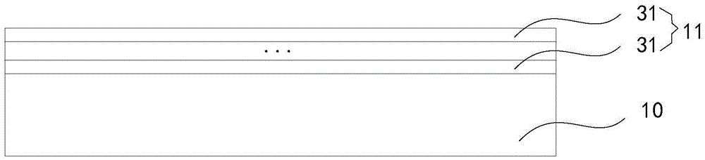
[0033] figure 2 A kind of AlN template provided by the first embodiment of the present invention is shown, such as figure 2 As shown, the AlN template includes a substrate 10 and an AlN thin film deposited on the substrate 10 . Wherein, the AlN thin film includes a first AlN layer 11 deposited on a substrate 10, and the first AlN layer 11 is doped with oxygen (O). Moreover, the oxygen content in the first AlN layer 11 gradually decreases from the interface between the first AlN layer 11 and the substrate 10 to the surface of the first AlN layer 11 .

[0034] Wherein, the substrate 10 includes but not limited to Si, SiC, sapphire, ZnO, GaAs, GaP, MgO, Cu and W substrates.

[0035]Part of the O atoms doped in the first AlN layer 11 ...


PUM

PropertyMeasurementUnit
thicknessaaaaaaaaaa
thicknessaaaaaaaaaa
thicknessaaaaaaaaaa

Abstract

The invention discloses an AlN template, a preparation method of the AlN template and a semiconductor device on the AlN template, and belongs to the field of semiconductor technology. The AlN template comprises a substrate and an AlN thin film deposited on the substrate. The AlN thin film comprises a first AlN layer deposited on the substrate. The first AlN layer is mixed with oxygen. The content of the oxygen in the first AlN layer is gradually reduced from an interface of the first AlN layer and the substrate to the surface of the first AlN layer. The semiconductor device comprises the AlN template and a nitride semiconductor layer. The AlN template comprises the substrate and the AlN thin film deposited on the substrate. The nitride semiconductor layer is deposited on the AlN thin film. The AlN template is the aforesaid AlN template. The method comprises steps of providing the substrate; and depositing the AlN thin film on the substrate. The AlN thin film comprises a first AlN layer deposited on the substrate. The first AlN layer is mixed with oxygen. The content of the oxygen in the first AlN layer is gradually reduced from an interface of the first AlN layer and the substrate to the surface of the first AlN layer.

Description

technical field [0001] The invention relates to the technical field of semiconductors, in particular to an AlN template, a preparation method of the AlN template and a semiconductor device on the AlN template. Background technique [0002] Currently, most GaN-based blue light emitting diodes (English: light emitting diode, abbreviation: LED) and GaN-based white light LEDs use sapphire substrates. Since sapphire and GaN materials have always had lattice mismatch and thermal mismatch problems, and there is only a small lattice mismatch between AlN materials, GaN materials, and sapphire substrates, AlN is placed on the sapphire substrate as a buffer layer and GaN. Specifically, an AlN buffer layer is first grown on a sapphire substrate to make an AlN template, and then GaN epitaxy is grown on the AlN template to make an LED epitaxial wafer. [0003] In the process of realizing the present invention, the inventor finds that there are at least the following problems in the prio...

Claims


Application Information

Patent Timeline
Patent Type & Authority Applications(China)
IPC IPC(8): H01L33/12H01L33/06H01L33/32H01L33/00
CPCH01L33/0066H01L33/0075H01L33/06H01L33/12H01L33/32
Inventor 董彬忠李鹏王江波
Owner HC SEMITEK SUZHOU
Why Eureka
Try Eureka