Encapsulation structure, electronic equipment and encapsulation method

A technology of packaging structure and packaging method, which is applied to circuits, electrical components, electric solid state devices, etc., can solve the problems of difficult process, high consumables, and high production cost, and achieves simple manufacturing process, high process difficulty, and low process difficulty. Effect

Active Publication Date: 2016-06-08
HUAWEI TECH CO LTD
View PDF4 Cites 25 Cited by
  • Summary
  • Abstract
  • Description
  • Claims
  • Application Information

AI Technical Summary

Problems solved by technology

[0004] It can be seen that the implementation scheme of 2.5DIC package in the prior art has the disadvantages of difficult process and high production cost
Moreover, the size of the silicon interposer is larger than the sum of all wafer sizes. The large-sized silicon interposer leads to high consumption (that is, high cost), which further increases the cost of 2.5DIC packaging, and is not conducive to the miniaturization of the packaging structure.

Method used


Image

  • Encapsulation structure, electronic equipment and encapsulation method
  • Encapsulation structure, electronic equipment and encapsulation method
  • Encapsulation structure, electronic equipment and encapsulation method

Examples


Embodiment Construction

[0041] The invention relates to a packaging structure and electronic equipment with the packaging structure, and also provides a packaging method for manufacturing the packaging structure. The following will clearly and completely describe the technical solutions in the embodiments of the present invention with reference to the drawings in the embodiments of the present invention.

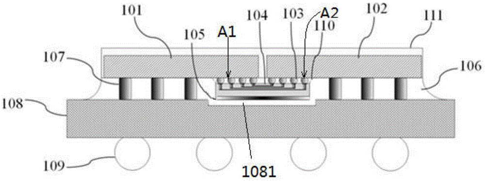
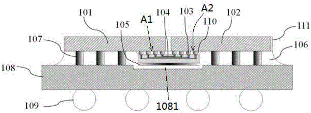
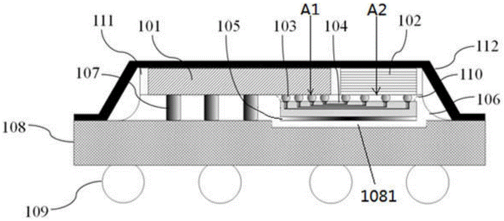
[0042] figure 1 Shown is a schematic diagram of the packaging structure provided by the first embodiment of the present invention. The packaging structure includes a substrate 108 , a fan-out unit 111 and a wiring layer 104 , and the fan-out unit 111 includes a first chip 101 and a second chip 102 . Please refer to Figure 7 , Figure 7 The structure of the fan-out unit 111 is schematically expressed, where hidden lines (lines that cannot be seen from the viewing direction) are indicated by dotted lines. The first chip 101 includes a first pin array A1, wherein the first pin array A1 includes a...


PUM


Abstract

The invention discloses an encapsulation structure which comprises a substrate, a fan-out unit and a wiring layer, wherein the fan-out unit comprises a first chip and a second chip; the first chip comprises a first pin array; the second chip comprises a second pin array; the fan-out unit also comprises a third pin array; the first pin array, the second pin array and the third pin array are opposite to the substrate; the wiring layer is bridged between the first pin array and the second pin array and used for connecting the first pins in the first pin array to corresponding second pin in the second pin array; the substrate is provided with a welding pad electrically connected with the wiring layer in the substrate; the third pin array is connected with the welding pad. The invention also discloses electronic equipment and an encapsulation method. The encapsulation structure disclosed by the invention has the advantages of low difficulty in production, low cost and miniaturization.

Description

technical field [0001] The invention relates to the technical field of microelectronic packaging, in particular to a packaging structure and a packaging method. Background technique [0002] With the continuous development of integrated electronic technology, the requirements for chip performance are also increasing, such as function enhancement, size reduction, energy consumption and cost reduction, etc., thus giving birth to 3DIC (three-dimensional integrated circuit) technology and 2.5DIC packaging technology. Silicon Interposer technology is a technical solution to realize the interconnection between wafers (Die) and the interconnection between wafers and substrates in three-dimensional integrated circuits and 2.5DIC packaging technologies. [0003] Taking the 2.5DIC package as an example, the 2.5DIC package in the prior art is to integrate at least two wafers into a fan-out unit (FanoutUnit) through the fan-out round-level packaging technology, and the fanout unit is pa...

Claims


Application Information

Patent Timeline
Patent Type & Authority Applications(China)
IPC IPC(8): H01L23/485H01L23/49H01L21/60
CPCH01L24/10H01L24/26H01L24/42H01L24/81H01L24/83H01L24/85H01L23/49H01L2224/1403H01L2924/15192H01L2924/15311H01L2224/16227H01L2224/32225H01L2224/73204H01L2224/73253H01L2924/15159H01L2924/16251H01L2924/3025H01L24/96H01L2224/12105H01L2224/73267H01L23/3675H01L23/5383H01L23/5385H01L23/485H01L2224/16225H01L2924/00H01L25/0655H01L24/14H01L24/06H01L23/367H01L21/563H01L23/3672H01L24/16
Inventor 赵南谢文旭张晓东符会利
Owner HUAWEI TECH CO LTD
Why Eureka
Try Eureka