Method for manufacturing flash memories

A manufacturing method and technology of flash memory devices, which are applied in the field of flash memory device manufacturing, can solve the problems that the yield rate of flash memory devices needs to be improved, and achieve the effect of small shape difference and good shape

Active Publication Date: 2016-06-15
SHANGHAI HUAHONG GRACE SEMICON MFG CORP
View PDF4 Cites 11 Cited by
  • Summary
  • Abstract
  • Description
  • Claims
  • Application Information

AI Technical Summary

Problems solved by technology

[0004] However, the yield rate of flash memory devices in the prior art needs to be improved

Method used


Image

  • Method for manufacturing flash memories
  • Method for manufacturing flash memories
  • Method for manufacturing flash memories

Examples


Embodiment Construction

[0023] It can be seen from the background art that the yield rate of flash memory devices formed in the prior art needs to be improved.

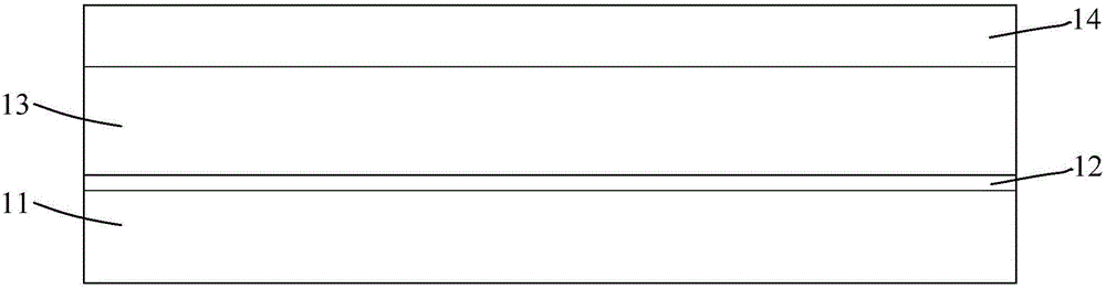
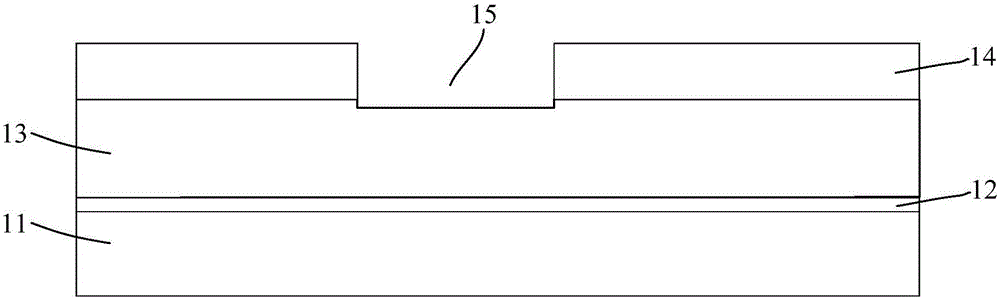
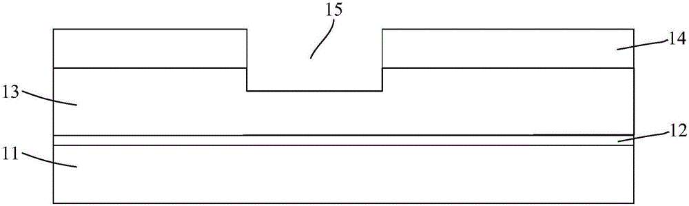
[0024] Figure 1 to Figure 5 It is a schematic cross-sectional structure diagram of a process of forming a flash memory device.

[0025] refer to figure 1 , providing a substrate 11, a coupling oxide (CouplingOxide) layer 12 on the substrate 11, a floating gate layer 13 on the coupling oxide layer 12, and a hard mask layer 14 on the floating gate 13;

[0026] refer to figure 2 , patterning the hard mask layer 14 to form an opening 15 penetrating through the hard mask layer 14 .

[0027] refer to image 3 , using the patterned hard mask layer 14 as a mask, using a first etching process to etch and remove the floating gate layer 13 with a first thickness along the opening 15 .

[0028] The semiconductor process is usually carried out with a lot as a unit. During the process of etching and removing the floating gate layer 13 of the first ...


PUM


Abstract

A method for manufacturing flash memories comprises the following steps: a graphical hard mask layer forms an opening penetrating a hard mask layer in a thickness direction; a floating gate layer with a first thickness below the opening is etched and removed with a first etching process, wherein etching time of the first etching process is determined based on the initial thickness of the floating gate layer below the opening before the first etching process, so that the thickness of the floating gate layer after the first etching process is completed is a fixed value; after the first etching process, a second etching process is adopted to etch and remove the floating gate layer with a second thickness, part of the floating gate layer below the hard mask layer is also etched and removed, and a floating gate tip region is formed below the hard mask layer, wherein the etching time of the second etching process is fixed. The method improves the morphological stability of formed floating gate tips, so that the yield of manufactured flash memories is improved.

Description

technical field [0001] The invention relates to the technical field of semiconductor manufacturing, in particular to a method for manufacturing a flash memory device. Background technique [0002] In the current semiconductor industry, integrated circuit products can be mainly divided into three types: analog circuits, digital circuits, and digital / analog hybrid circuits. Among them, memory devices are an important type of digital circuits. Among storage devices, the development of flash memory (Flash Memory, referred to as flash memory) is particularly rapid this year. The main feature of flash memory is that it can keep stored information for a long time without power on; and it has the advantages of high integration, fast storage speed, easy erasure and rewriting, etc., so it has been widely used in many fields such as microcomputer and automatic control. Wide range of applications. [0003] Flash memory devices mainly include a gate stack (StackGate) structure and a sp...

Claims


Application Information

Patent Timeline
Patent Type & Authority Applications(China)
IPC IPC(8): H01L21/8247H01L27/115H01L29/788H01L29/423H01L27/11521
CPCH01L29/42324H01L29/788H10B41/30
Inventor 徐涛曹子贵王卉陈宏
Owner SHANGHAI HUAHONG GRACE SEMICON MFG CORP
Why Eureka
Try Eureka