Light emitting diode and manufacturing method thereof

A technology of light-emitting diodes and two-dimensional electronic gas, which is applied to semiconductor devices, electrical components, circuits, etc., can solve problems such as unfavorable current lateral expansion, overheating breakdown of light-emitting devices, damage to MQW layer 20, etc., so as to improve local overheating vulnerability. Wear features, increase horizontal expansion ability, and improve the effect of antistatic ability

Active Publication Date: 2016-06-15
ANHUI SANAN OPTOELECTRONICS CO LTD
View PDF4 Cites 3 Cited by
  • Summary
  • Abstract
  • Description
  • Claims
  • Application Information

AI Technical Summary

Problems solved by technology

Due to the small contact area between the P electrode 70 and the epitaxial layer, when the device is working, the current tends to concentrate near the electrode, which is not conducive to the lateral expansion of the current, resulting in current congestion. Therefore, as the voltage increases, the area near the P electrode 70 Due to the congestion of the current in the area, it is easy to cause local overheating and breakdown of the light emitting device
At the same time, the growth temperature of the high-temperature P-type GaN layer 50 is 900-1050° C., which is relatively high, and will cause structural damage to the grown MQW layer 20 , and has a thickness of 40-300 nm, which has light absorption, thereby Reduced luminous efficiency of LED devices

Method used


Image

  • Light emitting diode and manufacturing method thereof
  • Light emitting diode and manufacturing method thereof
  • Light emitting diode and manufacturing method thereof

Examples


Embodiment Construction

[0027] The specific implementation manner of the present invention will be described in detail below with reference to the drawings and embodiments.

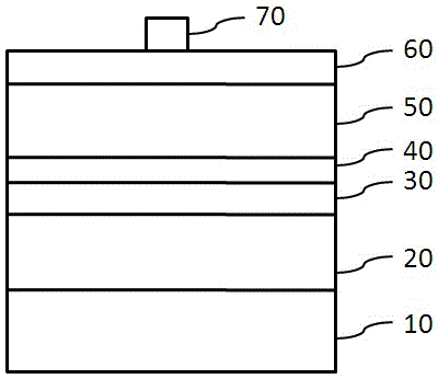
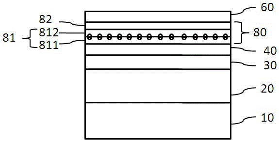
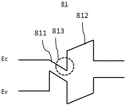
[0028] See attached figure 2 , a light-emitting diode designed in the present invention, at least including: N-type layer 10, active layer 20, low-temperature P-type GaN layer 40 located on active layer 20, non-P-type nitride layer 80 and P-type contact Layer 60, wherein the N-type impurity is any one of silicon, germanium, and tin, which is used to provide electrons, and the P-type impurity is any one of beryllium, magnesium, calcium, strontium, and barium, which is used to provide holes; The active layer 20 is a periodic structure composed of InGaN well layers and GaN barrier layers, and its period number is 4-12. The low-temperature P-type GaN layer 40 is a hole injection layer located on the active layer 20 , which reduces the migration distance of holes during effective recombination of electrons and holes and increases r...


PUM


Abstract

The invention belongs to the technical field of semiconductors, and particularly relates to a light emitting diode and a manufacturing method thereof. The light emitting diode at least comprises an N-type layer, an active layer and a low-temperature P-type GaN layer and a P-type contact layer located on the active layer. A non P-type nitride layer is inserted between the low-temperature P-type GaN layer and the P-type contact layer to replace a high-temperature P-type GaN layer, damages and light absorption to the lattice quality of a quantum well by high-temperature growth can be reduced, the high-density two-dimensional electron gas in the non P-type nitride layer increases the current lateral expansion capability, partial device over heat and easy breakdown features caused by current congestion are improved, and the antistatic ability of the LED device is enhanced.

Description

technical field [0001] The invention belongs to the technical field of semiconductors, and in particular relates to a light emitting diode and a preparation method thereof. Background technique [0002] Light-emitting diode (abbreviated as LED) is a semiconductor solid-state light-emitting device, which uses a semiconductor PN junction as a light-emitting structure. In recent years, the third-generation wide-bandgap semiconductor materials represented by GaN have received widespread attention and vigorous research. , has achieved remarkable advantages in the field of high-power electronic devices, and has made breakthrough progress in recent years. [0003] as attached figure 1 As shown, the traditional GaN-based light-emitting diode structure at least includes: N-type layer 10, active (MQW) layer 20, P-type electron blocking layer 30, low-temperature P-type GaN type 40, high-temperature P-type GaN layer 50 and P-type The contact layer 60 , and the P electrodes 70 respecti...

Claims


Application Information

Patent Timeline
Patent Type & Authority Applications(China)
IPC IPC(8): H01L33/06H01L33/14H01L33/32H01L33/00
CPCH01L33/0075H01L33/06H01L33/14H01L33/32
Inventor 黄文宾林兓兓张家宏
Owner ANHUI SANAN OPTOELECTRONICS CO LTD
Why Eureka
Try Eureka