Supercharge Your Innovation With Domain-Expert AI Agents!

Optically pumped light emitting device and preparation method of monolithically integrated optically pumped light emitting device

A light-emitting device, monolithic integration technology, applied in the direction of semiconductor devices, electrical components, circuits, etc., can solve the problems of not being able to meet the lighting industry, reduce compressive stress, and insufficient strength, so as to reduce compressive stress, reduce loss, and reduce production costs Effect

Active Publication Date: 2022-04-01
姜全忠
View PDF4 Cites 0 Cited by
  • Summary
  • Abstract
  • Description
  • Claims
  • Application Information

AI Technical Summary

Problems solved by technology

[0006] The existing optical pumping method still needs to be optimized and improved: first, the existing technology uses a plane-to-plane pumping method, and the intensity of the blue-violet light reaching the yellow-green-red quantum well is not high enough, and it is necessary to increase the free electrons excited by the blue-violet light. and the concentration of holes to ensure that the yellow-green-red light quantum wells have suitable quantum efficiency and luminous efficiency; secondly, from the current point of view, the single-crystal GaN substrate is still very expensive, and the output is low, which cannot meet the needs of the light-emitting industry. The design must take into account the use of sapphire substrates; however, due to the thermal expansion coefficient of sapphire is much larger (about 35%) than that of nitride, that is, the thermal expansion mismatch, during the growth and cooling process, there will be a large gap in the nitride. Large compressive stress (300-500 MPa), so the compressive stress must be effectively reduced; moreover, in order to fully absorb blue-violet light and convert it into yellow-green light or red light, the number of quantum wells must be large, so the consumption of indium organometallic sources will be become a problem

Method used


Image

  • Optically pumped light emitting device and preparation method of monolithically integrated optically pumped light emitting device
  • Optically pumped light emitting device and preparation method of monolithically integrated optically pumped light emitting device
  • Optically pumped light emitting device and preparation method of monolithically integrated optically pumped light emitting device

Examples


preparation example Construction

[0061] The preparation method of the above-mentioned monolithic integrated optically pumped light-emitting device includes the following steps:

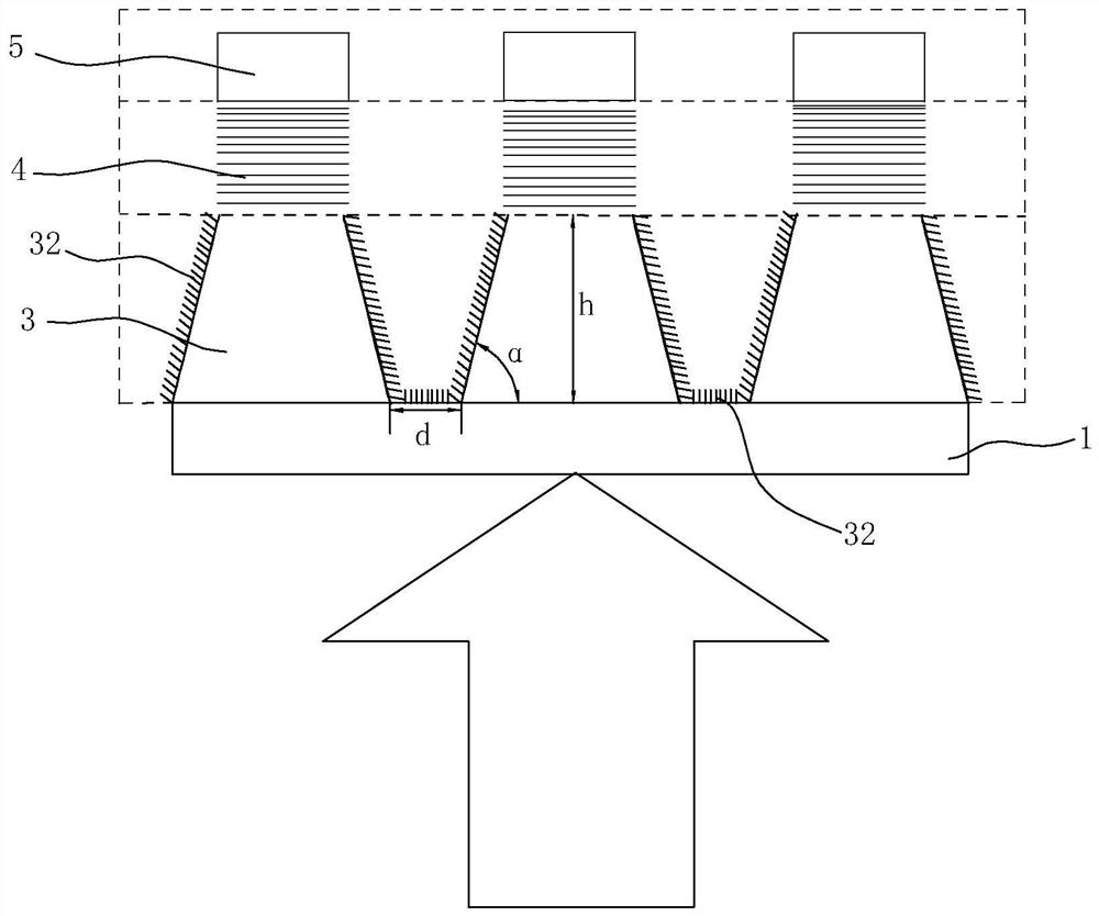
[0062] 1) Provide substrate 1: provide a cleaned single-sided polished substrate 1, the material of substrate 1 includes any one of these materials: (0001) surface sapphire, (0001) surface gallium nitride single crystal and (0001) surface aluminum nitride single crystal; when the unit body 3 is nitrogen polar, the substrate 1 is intentionally beveled, thereby deviating from the [0001] direction by 0-6°, and the deviating direction can be toward the (1-100) of the substrate 1 ) plane or (11-20) plane, or between the (1-100) plane and (11-20) plane facing the substrate 1; the thickness of the substrate 1 is preferably 0.4-5mm, and the transparency is preferably 385nm- In the 500nm spectral range, the transmittance is not lower than 60%; in this step, the double-sided polished substrate 1 cannot be used, because the polished other side ...

Embodiment 1

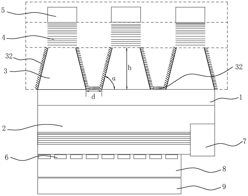
[0075] see image 3 with Figure 4 , In this embodiment, the substrate 1 is an undoped (0001) sapphire substrate with a thickness of 0.6mm.

[0076] The nitride structure 2 of the blue-violet light LED includes sequentially arranged from top to bottom: I) unintentionally doped GaN 2a, with a preferred thickness of 2 μm. It includes a 30nm GaN low-temperature nucleation layer; II) an n-type GaN layer 2b doped with Si, preferably with a thickness of 2.0 μm and a Si doping concentration of 3×10 +18 cm -3 ; III) Blue-violet light quantum well 2c, including 7 pairs, its composition is In x Ga 1-x N(0.01≤x≤0.30), preferably In 0.14 Ga 0.86 N(2nm) / Si:GaN(7nm), Si doping concentration is 1×10 +18 cm -3 and IV) Mg-doped p-type nitride layer 2d: its composition is Mg:Al 0.25 GaN 0.75 (10nm) / Mg:GaN, the preferred thickness is 350nm, and the Mg doping concentration is 3×10 +19 cm -3 . In this embodiment, the light emitting wavelength of the nitride structure 2 of the blue-vio...

Embodiment 2

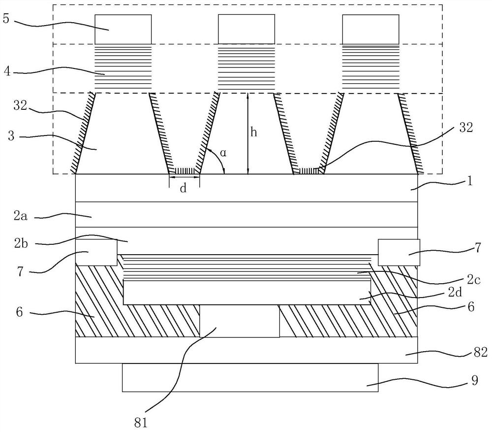
[0096] see Figure 5 with Image 6 , in this embodiment, the substrate 1 is an undoped beveled (0001) sapphire substrate with a thickness of 0.6 mm, the bevel rotation axis is [1-100], and the bevel angle is 1.2°. Chamfering helps reduce hexagonal surface defects during the growth of nitrogen-polar GaN required to form the unit body.

[0097] The nitride structure 2 of the blue-violet light LED includes sequentially arranged from top to bottom: I) unintentionally doped GaN 2a, preferably with a thickness of 2 μm, including GaN low-temperature nucleation layer (30nm); II) n-type doped Si The GaN layer 2b has a preferred thickness of 2.0 μm and a Si doping concentration of 3×10 +18 cm -3 ; III) blue-violet light quantum well 2c, including 7 pairs, its composition In 0.14 Ga 0.86 N(2nm) / Si:GaN(7nm), Si doping concentration is 1×10 +18 cm -3 and IV) Mg-doped P-type nitride layer 2d: its composition is Mg:Al 0.25 GaN 0.75 (10nm) / Mg:GaN, the preferred thickness is 350nm, an...


PUM

PropertyMeasurementUnit
angleaaaaaaaaaa
heightaaaaaaaaaa
heightaaaaaaaaaa

Abstract

The invention discloses an optically pumped light-emitting device, comprising a transparent substrate for nitride growth, a yellow-green-red quantum well structure, and a cover layer located above the yellow-green-red quantum well structure, characterized in that the substrate is characterized in that: A plurality of unit cells including but not limited to nitride are placed on one side, the unit cells have inclined sides, and the yellow-green-red quantum well structure is located on top of the unit cells. Also provided is a preparation method of the monolithically integrated optically pumped light-emitting device.

Description

technical field [0001] The invention relates to a light-pumped light-emitting device and a preparation method of a single-chip integrated light-pumped light-emitting device. Background technique [0002] High-efficiency and energy-saving InGaN / GaN quantum well light-emitting diodes (LEDs) are gradually replacing traditional light bulbs with high energy consumption and low luminous efficiency. However, this type of diode has low luminous efficiency in the yellow, green and red light bands, and the color is unstable. The reason is the compressive stress inside the light-emitting medium InGaN in the quantum well. This compressive stress mainly comes from lattice mismatch, that is, InGaN with a large lattice parameter grows on a GaN crystal plane with a small lattice parameter. Through the piezoelectric effect, a longitudinal electric field is formed. This electric field always separates the electrons from the holes in the InGaN quantum well, so they cannot recombine efficient...

Claims


Application Information

Patent Timeline
Patent Type & Authority Patents(China)
IPC IPC(8): H01L33/20H01L33/06
CPCH01L33/06H01L33/20H01L33/50
Inventor 姜全忠
Owner 姜全忠
Features
  • R&D
  • Intellectual Property
  • Life Sciences
  • Materials
  • Tech Scout
  • Unparalleled Data Quality
  • Higher Quality Content
  • 60% Fewer Hallucinations
Learn More