Optical waveguide, manufacturing method thereof, and method for reducing scattering loss of side wall of V-III semiconductor waveguide

A III-V, manufacturing method technology, applied in the direction of optical waveguide light guide, light guide, optics, etc., can solve the problems of restricting the resolution of single-chip integrated optical gyro, large refractive index difference, large scattering loss, and reduced yield, etc., to achieve high Sensitivity single-chip integrated optical gyroscope, overcome loss limitation, and reduce the effect of scattering loss

Active Publication Date: 2016-06-22
SUZHOU INST OF NANO TECH & NANO BIONICS CHINESE ACEDEMY OF SCI
View PDF8 Cites 0 Cited by
  • Summary
  • Abstract
  • Description
  • Claims
  • Application Information

AI Technical Summary

Problems solved by technology

This method makes the side wall roughness of the optical waveguide greatly dependent on each step of the process, so that the smoothness of the side wall is limited, and the cost of obtaining an optical waveguide with a truly smooth side wall increases and the yield decreases.
[0003] Large-scale and high-quality factor III-V semiconductor ring resonators are the basis and key to realize monolithic integrated optical gyro. For this large-scale III-V group ring resonator, due to the high refractive index of III-V semiconductors, large The large scattering loss caused by the difference in refractive index and the roughness of the side wall becomes the final factor restricting the improvement of its quality factor, which directly restricts the resolution of the monolithic integrated optical gyroscope.

Method used


Image

  • Optical waveguide, manufacturing method thereof, and method for reducing scattering loss of side wall of V-III semiconductor waveguide
  • Optical waveguide, manufacturing method thereof, and method for reducing scattering loss of side wall of V-III semiconductor waveguide
  • Optical waveguide, manufacturing method thereof, and method for reducing scattering loss of side wall of V-III semiconductor waveguide

Examples


Embodiment 1

[0029] The fabrication process of the low scattering loss waveguide is as follows:

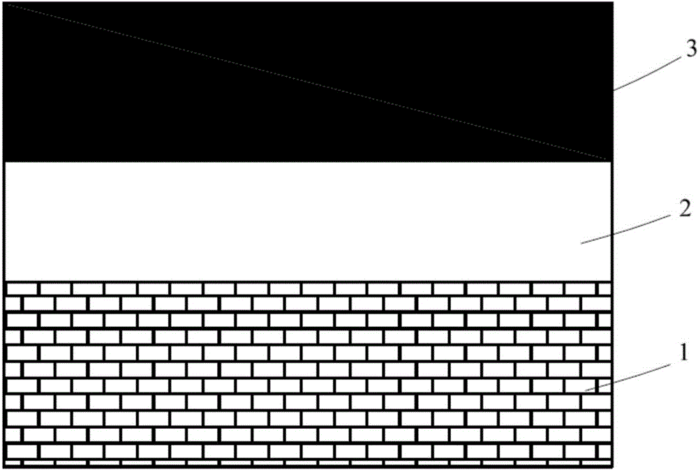
[0030] 1), reference Figure 1a As shown, the lower cladding layer 1, the core layer 2, and the upper cladding layer 3 are sequentially grown on the InP base material by MOCVD (or III-V semiconductor material growth methods such as MBE and HVPE), and the material of the lower cladding layer 1 is InP , the core layer 2 is a III-V semiconductor containing Al, its material is preferably InAlGaAs, and the material of the upper cladding layer is InP (or InGaAsP).

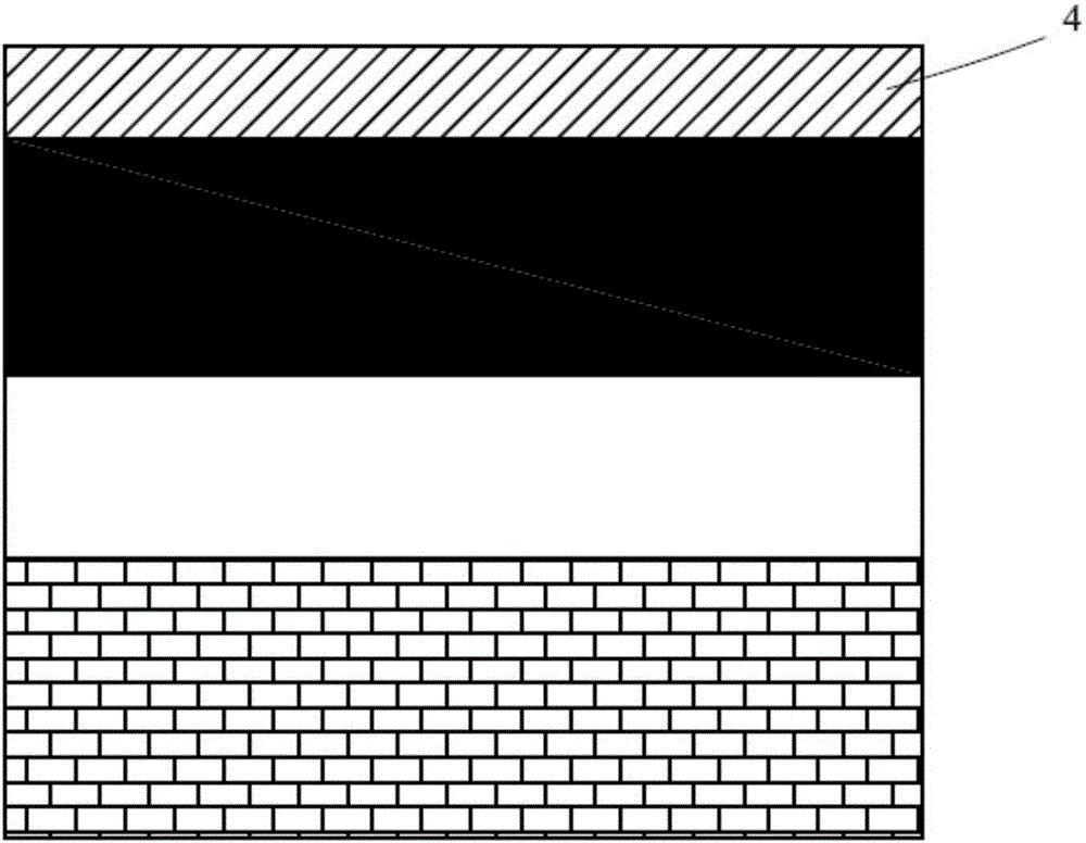
[0031] 2), reference Figure 1b As shown, a photoresist 4 is formed on the surface of the upper cladding layer by using a coater.

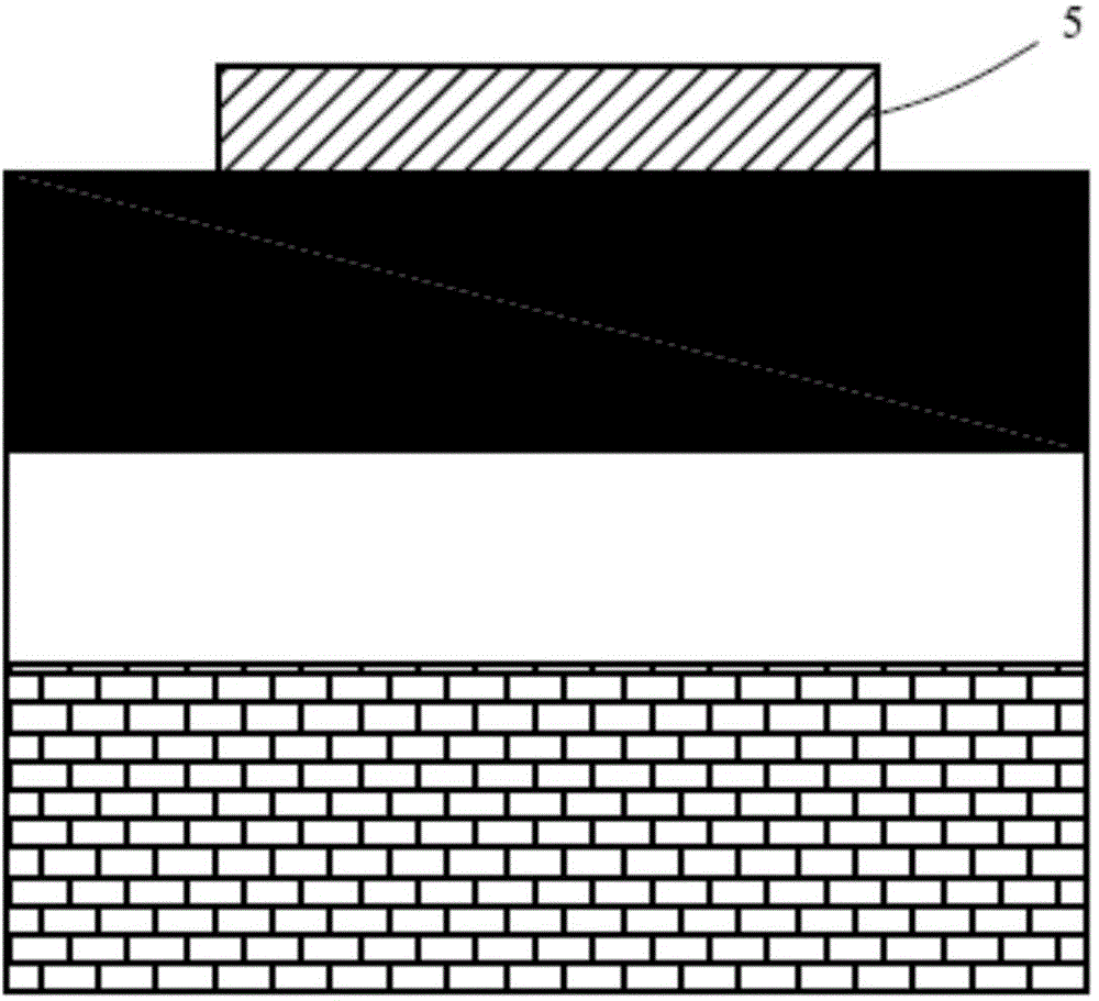
[0032] 3), reference Figure 1c As shown, a pattern mask 5 is obtained by photolithography.

[0033] 4), reference Figure 1d As shown, etching is carried out through the pattern mask 5 until the upper surface of the core layer 2 is exposed.

[0034] 5), reference Figure 1e As shown, the exposed part...

Embodiment 2

[0036] In step 4) of embodiment 1, it is also possible to etch through a pattern mask until the upper surface of the lower cladding layer is exposed, see Figure 2a As shown, aluminum oxidation is then performed on the exposed ends of the core layer to obtain an optical waveguide with smooth sidewalls, see Figure 2b shown.

Embodiment 3

[0038] ginseng image 3 As shown, the optical waveguide can also be a double-groove type, the upper cladding layer is photolithographically formed with two grooves 7, and the two grooves extend to the upper surface of the core layer, and the core layer at the bottom of the groove 7 is aluminum Oxidation can form smooth sidewalls between the oxidized core and the unoxidized core. Its preparation method is the same as that of Example 1, and will not be repeated here.


PUM

PropertyMeasurementUnit
refractive indexaaaaaaaaaa

Abstract

The invention relates an optical waveguide, a manufacturing method thereof, and a method for reducing the scattering loss of the side wall of a V-III semiconductor waveguide. The optical waveguide comprises a core layer; the surface of the core layer is coated with a limiting layer; the limiting layer comprises an aluminum oxide clad layer; and a smooth side wall is formed between the aluminum oxide clad layer and the core layer. According to the optical waveguide, the manufacturing method thereof, and the method for reducing the scattering loss of the side wall of the V-III semiconductor waveguide, an aluminum-containing V-III semiconductor is adopted as the core layer material of the optical waveguide; the optical waveguide is defined through aluminum oxidation; on the one hand, the aluminum oxidation-defined optical waveguide is realized, so that the aluminum-containing semiconductor is surround by a Al2O3 medium, and the refractive index difference of the aluminum-containing semiconductor and the Al2O3 medium is small, and therefore, the sensitivity of scattering loss to the roughness of the side wall of the waveguide is decreased, and on the other hand, an aluminum oxidation process is a wet oxidation technology, such kind of chemical reaction takes effect at the molecular level, and therefore, the roughness of the side wall of the waveguide structure defined by aluminum oxidation is undoubtedly far smaller than the roughness of the side wall of a waveguide structure defined by dry etching.

Description

technical field [0001] The present application relates to an optical waveguide and a manufacturing method thereof, and a method for reducing scattering loss on the side wall of a III-V semiconductor waveguide. Background technique [0002] Scattering loss caused by rough sidewalls is an insurmountable problem for all passive optical waveguides, especially for large-scale optical waveguides, which may become the ultimate limiting factor for their performance improvement. For the ridge waveguide defined by III-V materials, since the refractive index of III-V materials is greater than 3, while the refractive index of air is 1, the large refractive index difference makes its scattering loss very important to the sidewall roughness. Therefore, in order to reduce the waveguide scattering loss, the usual method is to obtain an optical waveguide structure with smooth side walls. Obtain high-quality optical waveguides. This method makes the sidewall roughness of the optical wavegui...

Claims


Application Information

Patent Timeline
Patent Type & Authority Applications(China)
IPC IPC(8): G02B6/122G02B6/13
Inventor 张瑞英
Owner SUZHOU INST OF NANO TECH & NANO BIONICS CHINESE ACEDEMY OF SCI
Why Eureka
Try Eureka