Wafer processing method

一种加工方法、晶片的技术,应用在金属加工设备、制造工具、适用于磨削工件平面的机床等方向,能够解决粘接膜破碎、飞散器件芯片品质、器件芯片品质降低等问题,达到抑制间隙的扩展、减少侧面污染、抑制移动的效果

Inactive Publication Date: 2016-06-22
DISCO CORP
View PDF7 Cites 9 Cited by
  • Summary
  • Abstract
  • Description
  • Claims
  • Application Information

AI Technical Summary

Problems solved by technology

[0011] However, if a protective tape is attached to the front surface of the wafer on which the modified layer is continuously formed along the planned division line, and the protective tape side is held on the chuck table, the back surface of the wafer is ground while grinding water. Forming it into a predetermined thickness and dividing the wafer into individual device chips thus has the following problem: grinding water invades from the gaps divided into individual device chips to contaminate the side and front surfaces of the device chips, thereby making the device chips reduced quality
[0012] Also, if an adhesive film is mounted on the back surface of a wafer that has been divided into individual device chips and a dicing tape is attached, and the adhesive film is broken along the individual device chips by expanding the dicing tape, there is a problem as follows : Since the adhesive film is formed slightly larger than the wafer, the outer peripheral portion of the adhesive film is broken and scattered and adheres to the front surface of the device chip, degrading the quality of the device chip

Method used


Image

  • Wafer processing method
  • Wafer processing method
  • Wafer processing method

Examples


Embodiment Construction

[0032] Hereinafter, preferred embodiments of the wafer processing method of the present invention will be described in detail with reference to the drawings.

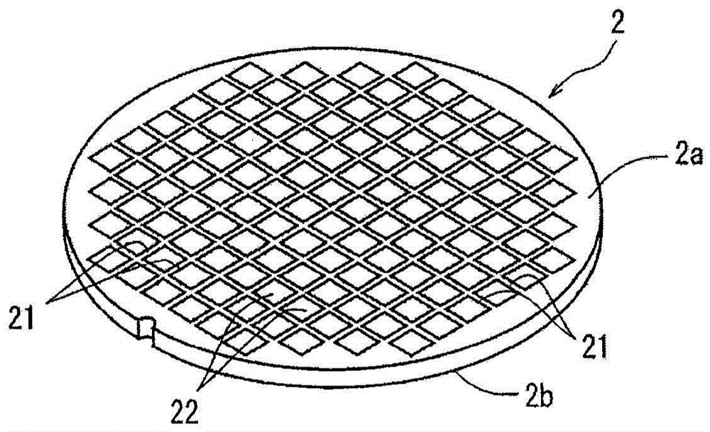
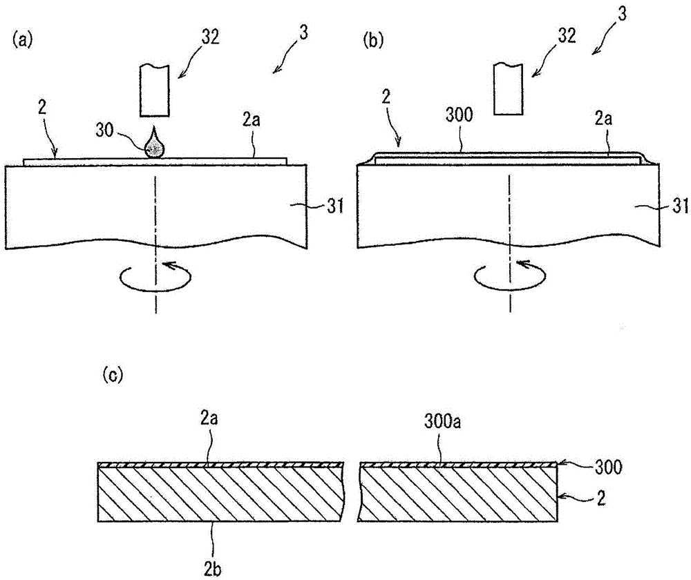
[0033] figure 1 A perspective view of a semiconductor wafer processed according to the invention is shown in . figure 1 The illustrated semiconductor wafer 2 is composed of a silicon wafer with a thickness of, for example, 500 μm. On the front surface 2 a, a plurality of planned dividing lines 21 are formed in a grid pattern, and are formed in a plurality of regions divided by the plurality of planned dividing lines 21 . There are devices 22 such as ICs and LSIs. Hereinafter, a wafer processing method for dividing the semiconductor wafer 2 into individual devices 22 along the planned dividing lines 21 will be described.

[0034] First, a protective film forming step is performed to form a protective film by coating the front surface 2 a of the semiconductor wafer 2 with a liquid resin that is hardened by irradiation o...


PUM


Abstract

A wafer processing method is provided. When a wafer is divided into various devices, implementation can be performed in a condition that side faces and front faces of the devices are not polluted. The wafer processing method comprises the following steps: a modified layer forming step that a converged spot is positioned in the wafer, a laser light ray having a permeable wavelength irradiates along a segment predetermined line, and then a modifier layer is formed in the wafer along the segment predetermined line; and a back face grinding step that grinding water is supplied on one and a back face is grinded at the same time so that a specified thickness is formed, and the wafer is divided into various device chips along the segment predetermined line taking the modified layer as a fracture starting point. The wafer processing method further comprises a protection film forming step that, before the back face grinding step is implemented, a liquid resin hardening caused by irradiation of ultraviolet light wraps the front face of the wafer, and then a protection film is formed; a protection film hardening step that the protection film is irradiated by the ultraviolet light to harden the protection film; and a protection tap bonding step that a protection tap is bonded to a surface of the protection film.

Description

technical field [0001] The present invention relates to a method of processing a wafer in which a plurality of planned dividing lines are formed in a grid pattern on the front surface, and devices are formed in a plurality of regions divided by the plurality of planned dividing lines, along which Divide the wafer. Background technique [0002] In the manufacturing process of semiconductor devices, a plurality of regions are divided by dividing lines arranged in a grid pattern on the front surface of a substantially disk-shaped semiconductor wafer, and devices such as ICs and LSIs are formed in the divided regions. The semiconductor wafer formed in this manner is cut along planned dividing lines to divide the regions where the devices are formed to manufacture individual device chips. [0003] The above-mentioned cutting along the planned dividing line of the semiconductor wafer is usually performed by a cutting device called a dicing saw. The cutting device has: a chuck ta...

Claims


Application Information

Patent Timeline
Patent Type & Authority Applications(China)
IPC IPC(8): H01L21/78B24B7/22
CPCH01L21/78H01L21/304H01L21/6836H01L2221/68327H01L2221/6834H01L2221/68386H01L2924/0002H01L2924/00B24B7/228
Inventor 中村胜松冈祐哉
Owner DISCO CORP
Why Eureka
Try Eureka