A turn-off performance improving method for an insulated gate bipolar transistor

A bipolar transistor and insulated gate technology, applied in semiconductor devices, electrical components, circuits, etc., can solve the problems of slow hole extraction speed, small turn-off energy loss, high turn-off energy loss, etc., to improve turn-off loss , low turn-off loss, and improved conduction voltage drop

Active Publication Date: 2016-06-22
SOUTHEAST UNIV
View PDF4 Cites 2 Cited by
  • Summary
  • Abstract
  • Description
  • Claims
  • Application Information

AI Technical Summary

Problems solved by technology

[0002] Insulated gate bipolar transistors need lower turn-on voltage drop and smaller turn-off energy loss in power supply, induction heating, electric traction and other power switching applications. For this reason, several innovative methods have been proposed in recent years Insulated gate bipolar transistor structure, for example, literature (1) [Y.Onozawa, "Development of the next generation1700Vtrench-gateFS-IGBT", Proceedingsofthe23 rd International Symposium on Power Semiconductor Devices and ICs, SanDiego, CA, May.2011, P52-55] proposed the traditional structure in this patent, which can obtain a very low turn-on voltage drop, but when it is turned off, due to the slow extraction speed of the accumulated holes, the turn-off Long off time, resulting in high turn-off energy loss

Method used


Image

  • A turn-off performance improving method for an insulated gate bipolar transistor
  • A turn-off performance improving method for an insulated gate bipolar transistor
  • A turn-off performance improving method for an insulated gate bipolar transistor

Examples


Embodiment 1

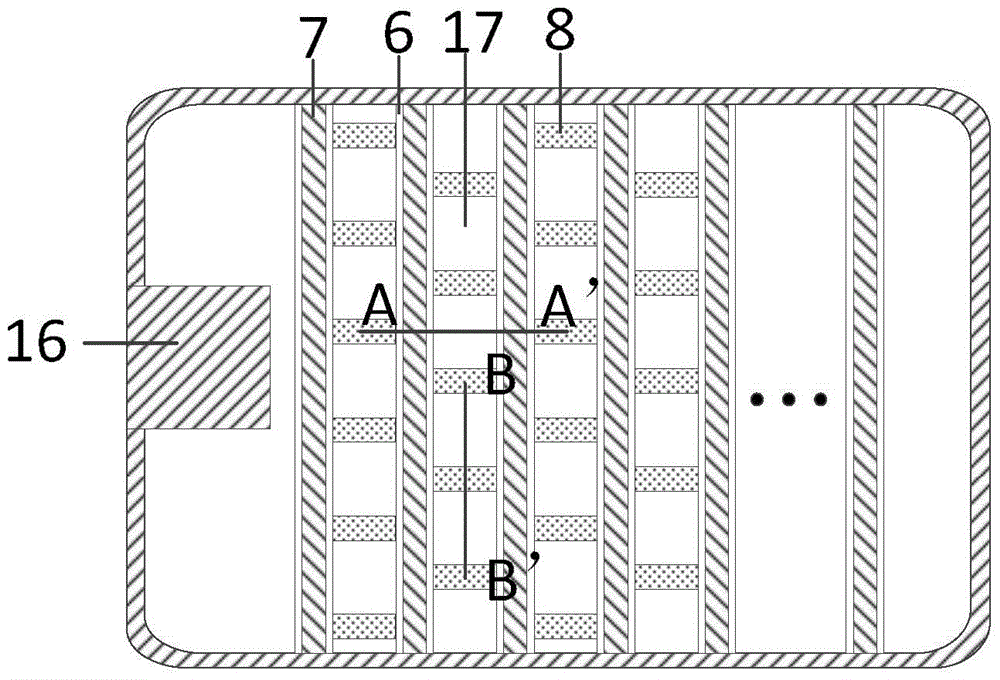
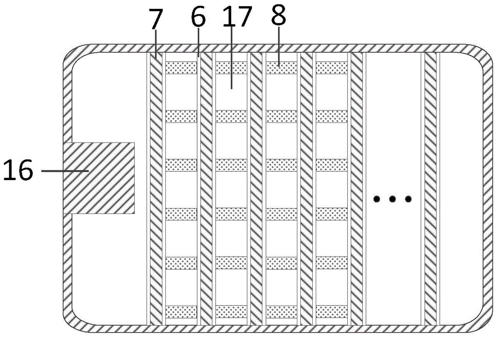
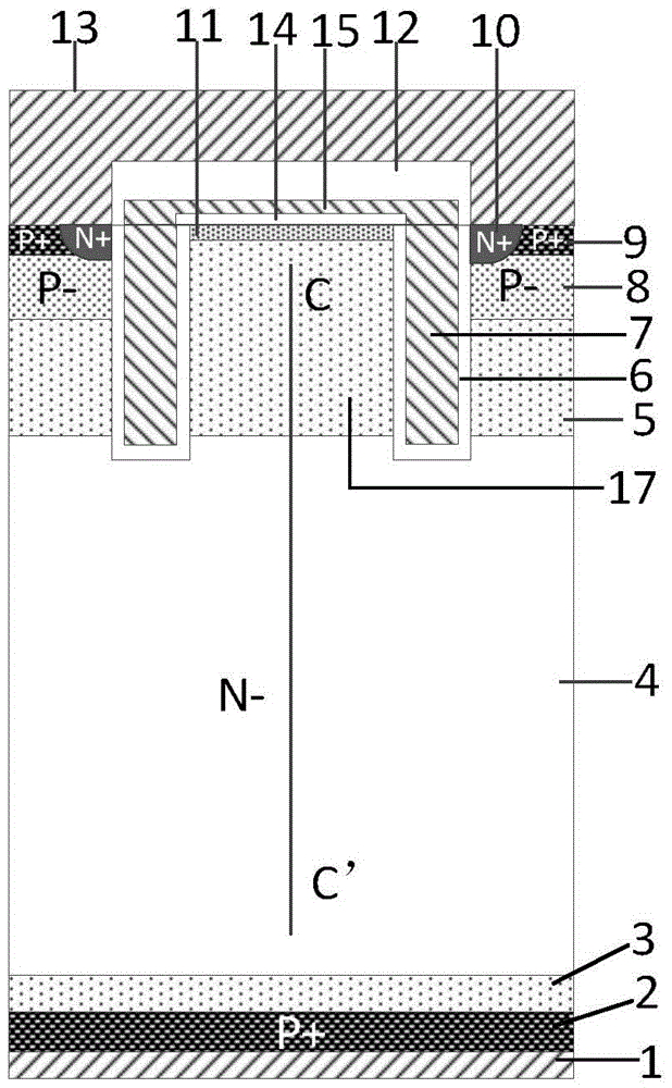
[0029]An insulated gate bipolar transistor, comprising: a heavily doped P-type collector region 2, a collector metal 1 is arranged on the back of the heavily doped P-type collector region 2, and a lightly doped N-type buffer is arranged on the front thereof Layer 3, the lightly doped N-type buffer layer 3 is provided with a lightly doped N-type base region 4, and the lightly doped N-type base region 4 is provided with a lightly doped N-type carrier storage layer 5. The doped N-type carrier storage layer 5 is provided with trench gates parallel to each other, the trench gates are composed of a first type gate oxide layer 6 and a first polysilicon gate 7, the first type gate oxide layer Layer 6 is located between the first polysilicon gate 7 and the lightly doped N-type carrier storage layer 5, the depth of the trench gate goes deep into the lightly doped N-type base region 4, and the trench gate will be lightly doped with N type carrier storage layer 5 is divided into strips, a...

Embodiment 2

[0036] A method for preparing an insulated gate bipolar transistor with improved turn-off performance, comprising:

[0037] The first step: first select N-type silicon material as the substrate and epitaxially grow shallowly doped N-type epitaxial layer;

[0038] The second step: ion implantation of N-type impurities, and annealing to form a lightly doped N-type carrier storage layer 5;

[0039] The third step: etching the trench, and forming the first type gate oxide layer 6 and the second type gate oxide layer 14;

[0040] Step 4: Deposit polysilicon, and etch to form the first polysilicon gate 7;

[0041] Step 5: Selective ion implantation of P-type impurities, and annealing to form a lightly doped P-type body region 8;

[0042] Step 6: ion implantation of P-type impurities, and annealing to form a lightly doped shallow P well 11;

[0043] Step 7: Deposit polysilicon to form a second polysilicon gate 15;

[0044] Step 8: selectively etching the light second polysilicon ...


PUM


Abstract

An insulated gate bipolar transistor structure comprises collector metal, a P-type collector region and an N-type base region. The surface of the N-type base region is provided with an N-type carrier storage layer and a groove gates. The groove gates divide the N-type carrier storage layer into strips. The surface of the strip-shaped N-type carrier storage layer is uniformly provided with block-shaped P-type body regions. The block-shaped carrier storage layer is provided with a second-type gate oxide layer connected to a first-type gate oxide layer. The second-type gate oxide layer is provided with a second polysilicon gate connected to a first polysilicon gate. The surfaces of the block-shaped P-type body regions are provided with P-type source regions and N-type source regions and are connected to emitter metal. The structure is characterized in that the surface of the block-shaped carrier storage layer is provided with light-doped shallow P-wells connected to the block-shaped P-type body regions. When the device in conduction, a grid electrode applies a positive grid voltage which is completely exhausted by the light-doped shallow P-wells to realize an injection efficiency enhance effect and enable the device to have a relatively small conduction pressure drop. When the device is turned off, the light-doped shallow P-wells are not completely exhausted, and conductive channels form to accelerate the device turn-off speed.

Description

technical field [0001] The invention mainly relates to the technical field of power semiconductor devices, in particular to a low-loss insulated gate bipolar transistor structure and a preparation method thereof, and is especially suitable for power supply, induction heating, electric traction and the like. Background technique [0002] Insulated gate bipolar transistors need lower turn-on voltage drop and smaller turn-off energy loss in power supply, induction heating, electric traction and other power switching applications. For this reason, several innovative methods have been proposed in recent years Insulated gate bipolar transistor structure, for example, literature (1) [Y.Onozawa, "Development of the next generation1700Vtrench-gateFS-IGBT", Proceedingsofthe23 rd International Symposium on Power Semiconductor Devices and ICs, SanDiego, CA, May.2011, P52-55] proposed the traditional structure in this patent, which can obtain a very low turn-on voltage drop, but when it ...

Claims


Application Information

Patent Timeline
Patent Type & Authority Applications(China)
IPC IPC(8): H01L29/739H01L29/06
CPCH01L29/0603H01L29/7393
Inventor 祝靖周锦程杨卓孙伟锋宋慧滨陆生礼时龙兴
Owner SOUTHEAST UNIV
Why Eureka
Try Eureka