Shield grid trench MOSFET device and manufacturing method thereof

A technology of shielded gate and trench, which is applied in the manufacture of shielded gate trench MOSFET devices, and in the field of shielded gate trench MOSFET devices, can solve the problems that the device unit cannot be effectively reduced, the consistency of the device is deteriorated, and the manufacturing process is complicated. Achieve the effects of easy control, reduced stepping, and reduced manufacturing difficulty

Active Publication Date: 2016-06-22
SHENZHEN SANRISE TECH CO LTD
View PDF4 Cites 23 Cited by
  • Summary
  • Abstract
  • Description
  • Claims
  • Application Information

AI Technical Summary

Problems solved by technology

[0010] figure 1 In the shielded gate structure of the existing structure shown, the shielding dielectric film needs to reach a certain thickness to withstand the source-drain voltage. Generally, for a 100V device, the thickness on the sidewall needs to be 5000-6000 angstroms, so that the device unit cannot Effectively shrink, cannot use higher drift region impurity concentration to reduce on-resistance
At the same time, for such a device structure, after the bottom shielding dielectric film and the shielding electrode are completed, the device gate oxide film is grown. The manufacturing process is complicated. The influence of multiple factors such as film etching leads to poor device consistency

Method used


Image

  • Shield grid trench MOSFET device and manufacturing method thereof
  • Shield grid trench MOSFET device and manufacturing method thereof
  • Shield grid trench MOSFET device and manufacturing method thereof

Examples


Embodiment Construction

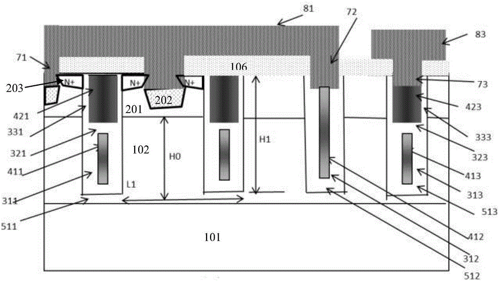
[0064] Such as figure 2 Shown is the layout of the shielded gate trench MOSFET device in the first embodiment of the present invention; as Figure 3A Shown is the first embodiment of the present invention shielded gate trench MOSFET device along figure 2 The section view of the BB' position in ; such as Figure 3B Shown is the first embodiment of the present invention shielded gate trench MOSFET device along figure 2 The cross-sectional view of the AA' position in the figure; the shielded gate trench MOSFET device in the first embodiment of the present invention is described by taking an N-type device as an example, that is, in the first embodiment of the present invention, the first conductivity type is N-type, and the second The conductivity type is P-type; the structure of the P-type device can be obtained by exchanging the doped conductivity type of the device between N-type and P-type, and the description of the present invention does not describe the P-type device i...


PUM


Abstract

The invention discloses a shield grid trench MOSFET device.In grid electrode structures of primitive cells, shield electrodes are formed after epitaxial layers filling trenches are etched back, and trench grids are formed at the tops of the shield electrodes; the shield electrodes and adjacent drift regions make direct contact, carrier balance is achieved, the shield electrodes of the primitive cells and the drift regions form alternately-arranged structures in the transverse direction, and the shield electrodes carry out transverse exhausting on the adjacent drift regions in reverse bias of the device.The invention further discloses a manufacturing method of the shield grid trench MOSFET device.According to the shield grid trench MOSFET device and the manufacturing method, it is unnecessary to arrange dielectric films at the bottoms of the shield electrodes, stepping of device units can be reduced, the specific on-resistance of the device can be reduced, manufacturing difficulty can be lowered, and the uniformity of device performance can be improved.

Description

technical field [0001] The invention relates to the field of manufacturing semiconductor integrated circuits, in particular to a shielded gate trench MOSFET device; the invention also relates to a manufacturing method of the shielded gate trench MOSFET device. Background technique [0002] Such as figure 1 As shown, it is a schematic structural diagram of an existing shielded gate trench MOSFET device; the current flow region of the existing shielded gate trench MOSFET device is composed of a plurality of primitive cells arranged periodically, each of which includes: [0003] An N-type epitaxial layer 102 formed on the surface of a semiconductor substrate such as a silicon substrate 101, a trench 511 is formed in the N-type epitaxial layer 102, the shielding electrode 411 is composed of polysilicon filled at the bottom of the trench 511, and the trench gate 421 It is composed of polysilicon filled on the top of the trench 511; a shielding dielectric film 311 is isolated bet...

Claims


Application Information

Patent Timeline
Patent Type & Authority Applications(China)
IPC IPC(8): H01L29/78H01L21/336H01L29/423H01L21/28
CPCH01L21/28008H01L29/4236H01L29/66477H01L29/78
Inventor 肖胜安
Owner SHENZHEN SANRISE TECH CO LTD
Why Eureka
Try Eureka