Carbon nanotube thin film, device comprising thin film, carbon nanotube thin film manufacture method and carrier substrate

A carbon nanotube thin film and carrier substrate technology, which is applied in the manufacture of electrical solid state devices, semiconductor devices, semiconductor/solid state devices, etc., can solve the problems of reduced productivity and long carbon nanotube thin film preparation cycle, etc.

Inactive Publication Date: 2016-06-22
BOE TECH GRP CO LTD
View PDF6 Cites 3 Cited by
  • Summary
  • Abstract
  • Description
  • Claims
  • Application Information

AI Technical Summary

Problems solved by technology

[0005] In the prior art, the above-mentioned carbon nanotube film can usually be prepared by standing and volatilizing the solution. Since the standing process takes a long time, the preparation cycle of the above-mentioned method for preparing the carbon nanotube film is relatively long, which reduces the productivity.

Method used


Image

  • Carbon nanotube thin film, device comprising thin film, carbon nanotube thin film manufacture method and carrier substrate
  • Carbon nanotube thin film, device comprising thin film, carbon nanotube thin film manufacture method and carrier substrate
  • Carbon nanotube thin film, device comprising thin film, carbon nanotube thin film manufacture method and carrier substrate

Examples


Embodiment Construction

[0036] The following will clearly and completely describe the technical solutions in the embodiments of the present invention with reference to the accompanying drawings in the embodiments of the present invention. Obviously, the described embodiments are only some, not all, embodiments of the present invention. Based on the embodiments of the present invention, all other embodiments obtained by persons of ordinary skill in the art without making creative efforts belong to the protection scope of the present invention.

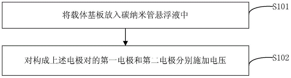
[0037] Embodiments of the present invention provide a method for preparing a carbon nanotube film, such as figure 1 shown, including:

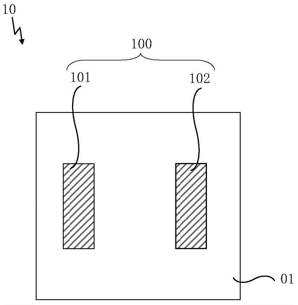
[0038] S101, as figure 2 The shown carrier substrate 10 is placed in a suspension of carbon nanotubes.

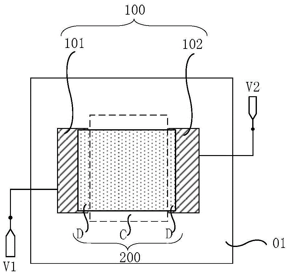
[0039] Wherein, the carrier substrate 10 includes a first base substrate 01 and electrode pairs 100 formed on the first base substrate 01 . The electrode pair 100 includes a first electrode 101 and a second electrode 10...


PUM


Abstract

An embodiment of the invention provides a carbon nanotube thin film, a device comprising the thin film, a carbon nanotube thin film manufacture method and a carrier substrate and relates to the technical field of display technologies, and efficiency of manufacturing the carbon nanotube thin film with carbon nanotube solutions can be improved. The carbon nanotube thin film manufacture method comprises a first step of placing the carrier substrate into a carbon nanotube suspension liquid, wherein the carrier substrate comprises a first underlayment substrate and an electrode pair formed on the first underlayment substrate, and the electrode pair comprises a first electrode and a second electrode which are arranged opposite to each other. The carbon nanotube thin film manufacture method comprises a second step of respectively applying voltages on the first electrode and the second electrode that make up the electrode pair so as to form an electric field between the first electrode and the second electrode, wherein under the effect of the electric field, carbon nanotubes in the carbon nanotube suspension liquid gather on the surface of one side, provided with the electrode pair, of the first underlayment substrate so as to form a carbon nanotube thin film.

Description

technical field [0001] The invention relates to the field of display technology, in particular to a carbon nanotube film, a device containing the film, a preparation method, and a carrier substrate. Background technique [0002] A TFT (Thin Film Transistor, Thin Film Field Effect Transistor) is usually arranged on the array substrate of the LCD (Liquid Crystal Display, liquid crystal display) and in the pixel driving circuit of the AMOLED (Active Matrix Organic Light Emitting Diode, active driving organic light emitting diode) display. [0003] The material of the TFT active layer mainly includes two kinds of amorphous silicon (a-Si) and polycrystalline silicon (Poly-Si). Among them, amorphous silicon has low cost and simple process, but its mobility is low, which makes it difficult to meet the light-emitting requirements of OLED devices. However, the polysilicon process is complex and is limited by complex equipment such as ion implantation and laser crystallization. In ad...

Claims


Application Information

Patent Timeline
Patent Type & Authority Applications(China)
IPC IPC(8): H01L51/05H01L27/28H01L51/30H01L51/40
CPCH10K19/10H10K71/125H10K85/221H10K10/462
Inventor 张方振惠官宝高涛宁策
Owner BOE TECH GRP CO LTD
Why Eureka
Try Eureka