

High-speed semiconductor laser with beam diffusion structure
A diffusion structure and laser technology, applied in semiconductor lasers, optical waveguide semiconductor structures, lasers, etc., can solve the problems of burning semiconductor lasers and laser end face damage, and achieve the effects of suppressing diffusion, good mode matching, and reducing optical power density.
- Summary
- Abstract
- Description
- Claims
- Application Information
AI Technical Summary
Problems solved by technology
Method used
Image

Examples
Embodiment Construction
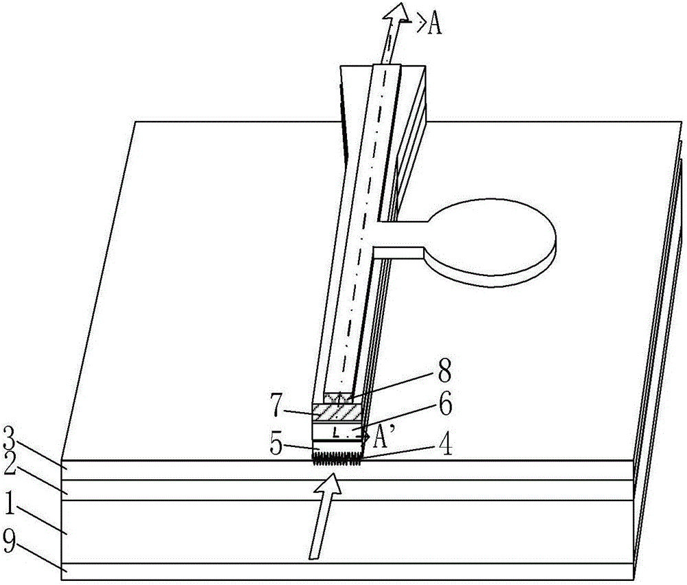
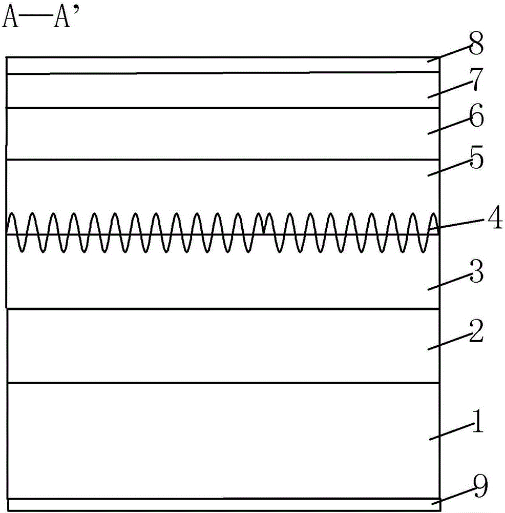
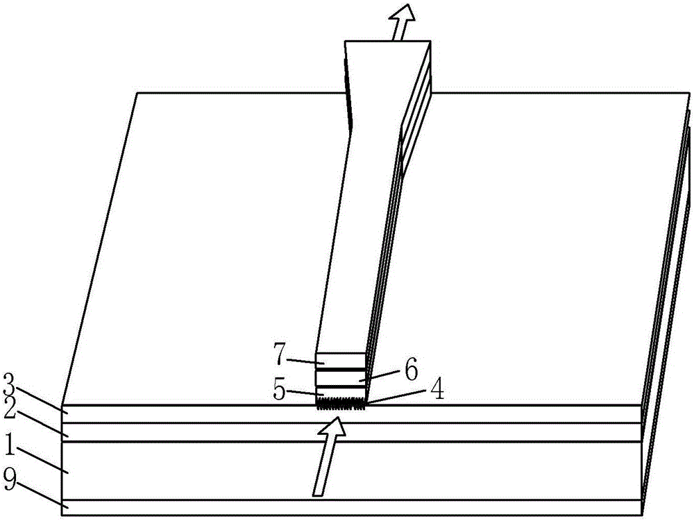
[0024] In order to achieve the above object, the present invention provides a high-speed semiconductor laser with a beam diffusion structure on the light emitting end surface. Specifically, it includes an optical waveguide structure, the optical waveguide structure includes a lower waveguide layer, a multi-quantum well active layer and an upper waveguide layer stacked in sequence from bottom to top, and the multi-quantum well active layer in the multi-quantum well active layer A grating layer is formed on the upper part. The upper waveguide layer is formed as a convex ridge, and has a beam diffusing structure on the side of the light-emitting end surface. The so-called beam diffusion structure means that for a laser with a resonant cavity length L, the projection of the light incident surface and the light exit surface on the Bragg grating has two mutually parallel sides, and the sides of the two mutually parallel sides The lengths are not equal, and the length direction of t...
PUM
| Property | Measurement | Unit |
|---|---|---|
| Length | aaaaa | aaaaa |
Abstract
Description
Claims
Application Information