Electromagnetic wave shielding composite film

A composite film and electromagnetic wave technology, applied in the direction of magnetic/electric field shielding, electrical components, etc., can solve the problems of ineffective shielding of low-frequency electromagnetic waves, high equipment investment costs, etc., and achieve the effect of improving electromagnetic wave shielding effect, light weight, and saving thickness

Active Publication Date: 2016-07-06
XSENSE TECH CORP
View PDF9 Cites 6 Cited by
  • Summary
  • Abstract
  • Description
  • Claims
  • Application Information

AI Technical Summary

Problems solved by technology

However, this conductive adhesive film method has the disadvantages of relatively expensive research and development and equipment investment costs and the inability to effectively shield low-frequency electromagnetic waves

Method used


Image

  • Electromagnetic wave shielding composite film
  • Electromagnetic wave shielding composite film
  • Electromagnetic wave shielding composite film

Examples


Embodiment 1

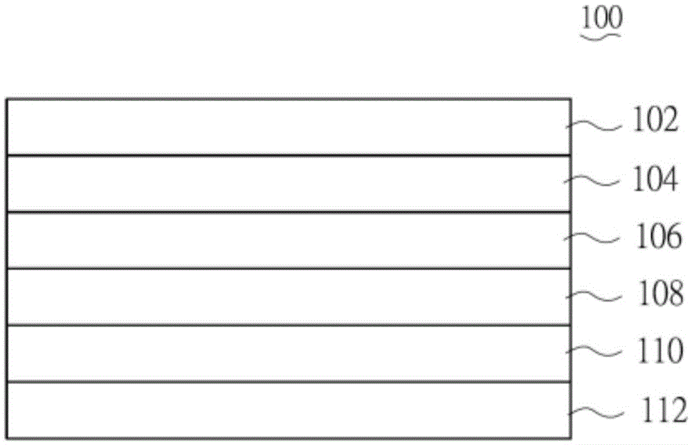
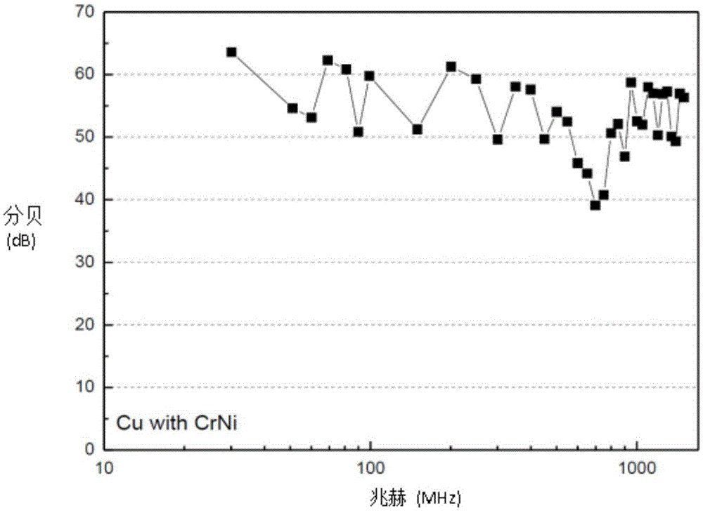
[0029] The electromagnetic shielding composite film of the present embodiment is completed by the following process steps: graphene is prepared by Mechanical Exfoliation, and its average thickness range can be from 0.2 nanometers to 300 nanometers, and then graphene (25% by weight), low Viscosity macromolecular binder (40 weight percent epoxy resin), hardener (15 weight percent polyamide hardener), dispersant (0.5 weight percent anionic dispersant), organic solvent (19 weight percent methyl ethyl ketone , a mixed solvent of toluene and ethyl acetate) and additives (0.5 weight percent defoamer), etc., are fully and evenly mixed, and coated and dispersed on the surface of the PET release film 112 to form an incident layer with a high conductive function 110, the thickness of which is about 15 micrometers; then, a wave-absorbing layer 108 of nickel-chromium alloy with a thickness of 50 nanometers and a reflective layer 106 of copper metal with a thickness of 300 nanometers are seq...

Embodiment 2

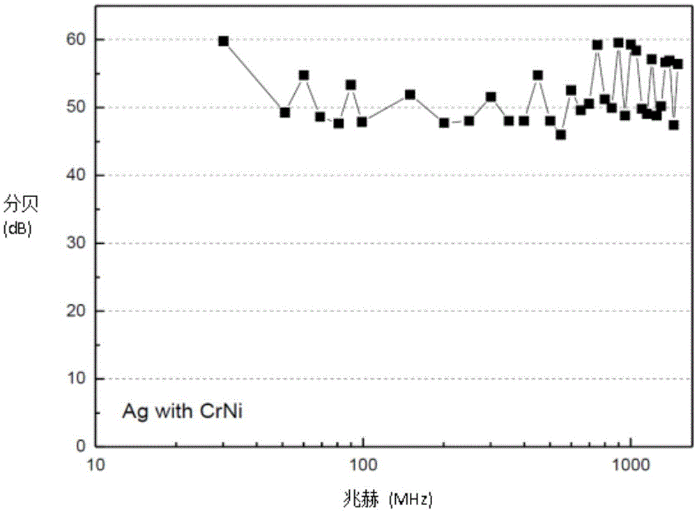
[0031] The electromagnetic shielding composite film of the present embodiment is completed by the following process steps: graphene is prepared by Mechanical Exfoliation, and its average thickness range can be from 0.2 nanometers to 300 nanometers, and then graphene (25% by weight) and low Viscosity macromolecular binder (40 weight percent epoxy resin), hardener (15 weight percent polyamide hardener), dispersant (0.5 weight percent anionic dispersant), organic solvent (19 weight percent methyl ethyl ketone , a mixed solvent of toluene and ethyl acetate) and additives (0.5 weight percent defoamer), etc., are fully and evenly mixed, and coated and dispersed on the surface of the PET release film 112 to form an incident layer with a high conductive function 110, the thickness of which is about 15 micrometers; then, a wave-absorbing layer 108 of nickel-chromium alloy with a thickness of 50 nanometers and a reflective layer 106 of silver metal with a thickness of 200 nanometers are ...

Embodiment 3

[0033] The electromagnetic shielding composite film of the present embodiment is completed by the following process steps: graphene is prepared by Mechanical Exfoliation, and its average thickness range can be from 0.2 nanometers to 300 nanometers, and then graphene (25% by weight) and low Viscosity macromolecular binder (40 weight percent epoxy resin), hardener (15 weight percent polyamide hardener), dispersant (0.5 weight percent anionic dispersant), organic solvent (19 weight percent methyl ethyl ketone , a mixed solvent of toluene and ethyl acetate) and additives (0.5% by weight defoamer) etc. are fully and evenly mixed and coated and dispersed on the surface of the PET release film 112 to form an incident layer 110 with a high conductive function. The thickness is about 15 microns; then, a wave-absorbing layer 108 of nickel-chromium alloy with a thickness of 50 nanometers and a reflective layer 106 of aluminum metal with a thickness of 300 nanometers are sequentially forme...


PUM


Abstract

The present invention discloses an electromagnetic wave shielding composite film, which is structurally characterized by comprising a multi-layer wave-absorbing structure. The structure at least includes a reflecting layer, a wave-absorbing layer and an incident layer. The resistance value of the wave-absorbing layer is higher than the resistance value of the reflecting layer. Electromagnetic waves are guided to drift back and forth between the wave-absorbing layer and the reflecting layer, so that energy attenuation of spatially incident electromagnetic waves is facilitated. Meanwhile, reflected electromagnetic waves are reduced or eliminated. Therefore, the electromagnetic wave shielding composite film has a multi-layer wave-absorbing structure, so that the interference of electromagnetic waves on adjacent lines and components is avoided. In addition, the thickness of the multi-layer wave-absorbing structure is thinned. As a result, the requirements of flexible circuit boards, such as light weight, thinned material and good flexibility, can be met.

Description

technical field [0001] The invention relates to an electromagnetic wave shielding composite film, in particular to an electromagnetic wave shielding composite film with a multi-layer wave-absorbing structure. Background technique [0002] In order to respond to the multi-functional market demand of electronic and communication products, the IC structure of the circuit substrate needs to be lighter, thinner, shorter, and smaller; in terms of function, it needs to be powerful and high-speed signal transmission. Therefore, the density of the number of I / O pins is bound to increase, and the number of IC pins must also increase accordingly. The distance between the IC substrate lines is getting closer and closer, and the operating frequency is moving towards high-bandwidth, which makes the electromagnetic interference (Electromagnetic Interference; EMI) between ICs more and more serious. Therefore, how to effectively manage the electromagnetic compatibility (Electromagnetic Compa...

Claims


Application Information

Patent Timeline
Patent Type & Authority Applications(China)
IPC IPC(8): H05K9/00
CPCH05K9/0088
Inventor 刘伟仁范晏宁沈骏
Owner XSENSE TECH CORP
Why Eureka
Try Eureka