
Method for embedding micro-ring resonator into D-shaped optical fiber

A technology of micro-ring resonator and optical fiber, which is applied in the field of optoelectronics, can solve problems such as inability to control, and achieve the effect of flat bandwidth and increased integration

Inactive Publication Date: 2016-07-13
HENAN UNIV OF SCI & TECH
View PDF6 Cites 0 Cited by
  • Summary
  • Abstract
  • Description
  • Claims
  • Application Information

AI Technical Summary

Problems solved by technology

But the disadvantage is that the existing waveguide resonant ring can only correspond to one wavelength, and cannot be adjusted according to actual parameters, and further improvement is urgently needed

Method used


Image

  • Method for embedding micro-ring resonator into D-shaped optical fiber
  • Method for embedding micro-ring resonator into D-shaped optical fiber
  • Method for embedding micro-ring resonator into D-shaped optical fiber

Examples


Embodiment 1

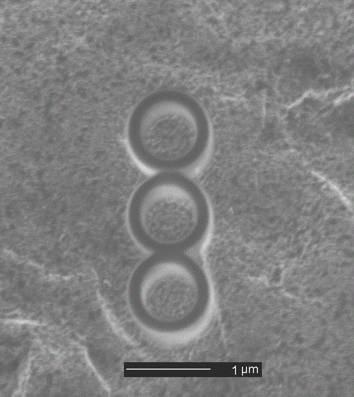
[0031] A method for embedding a microring resonator in a D-shaped optical fiber, comprising the steps of:

[0032] (1) Use silica gel to fix the curved part of the D-shaped fiber in a V-shaped groove. The V-shaped groove is 70 microns deep and 127 microns at the widest point. Partially coated with photoresist AZ-1350 and dried;

[0033] (2) Install the dried D-shaped optical fiber and the mask plate on the photolithography machine. The mask plate has slits with a single-peak pattern, and the peak width of the single-peak pattern is 3-10 microns. The peak height is 30 microns, the direction of the peak is along the fiber core direction of the optical fiber, the symmetry axis of the single peak coincides with the midline of the D-shaped optical fiber plane part, and then, the plane part of the D-shaped optical fiber is exposed by a mask plate, The purpose of exposure is to make the photoresist in the photosensitive area of ​​the D-shaped optical fiber plane part through the sli...

Embodiment 2

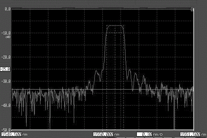
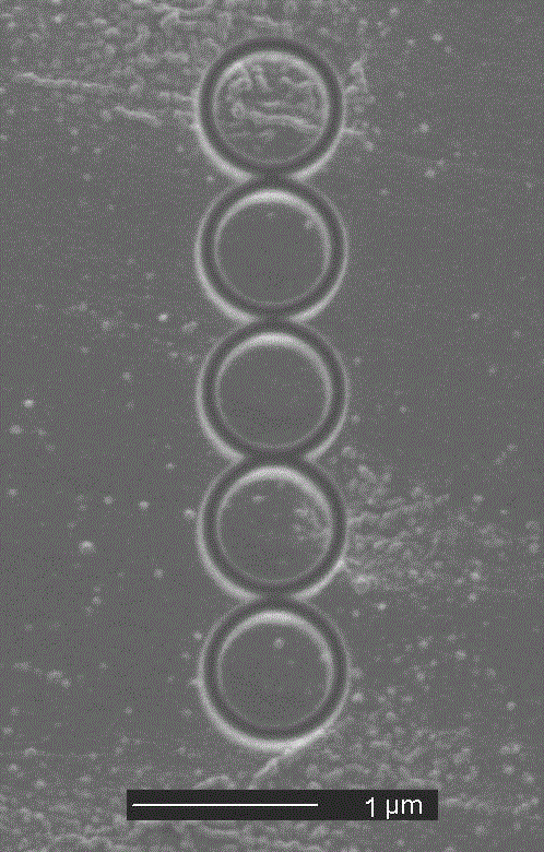
[0038] Steps refer to Example 1. The difference from Example 1 is that step (4) uses focused ion etching to process five cascaded microring resonators. The etched microring resonator structure is as follows image 3 shown. Figure 4 is the transmission spectrum figure of the structure of embodiment 2, by Figure 4 It can be seen that there is an obvious resonance effect at the wavelength of 1549.80-1550.10 nanometers (nm), not only has the characteristics of embodiment 1, but also the spectral line resonance peaks of the 5 resonant rings are sharper, this effect can be used in optical fiber narrowband filters Get valuable applications on it. It can be seen from the calculation that the Q value (quality factor) of the five cascaded resonant microcavities is 3.9×10 5. It shows that with the increase of cascaded resonant microrings, a higher quality factor can be obtained.


PUM


Abstract

The invention provides a method for embedding a micro-ring resonant cavity into a D-shaped optical fiber. The method includes the following steps that, 1 the curved surface part of the D-shaped optical fiber is fixed, and the plane part of the D-shaped optical fiber is coated with photoresist and dried; 2, the optical fiber obtained in step 1 is mounted on a lithography machine, the plane part of the D-shaped optical fiber is subjected to exposure through a mask plate, and the exposure position is the midcourt line of the plane part of the D-shaped light fiber; 3, the D-shaped optical fiber obtained in step 2 is immersed in acetone for development after being heated with a drying machine so as to remove photoresist at the exposure position, and the midcourt line position of the plane part of the D-shaped optical fiber can be marked with a pattern on the mask plate; 4, a micro-ring resonant cavity or multiple cascaded micro-ring resonant cavities are etched in the plane part of the D-shaped optical fiber obtained in step 3 through a focusing ion etching method, and the circle centers of the micro-ring resonant cavities are located at the midcourt line position of the plane part. According to the method, the micro-ring resonant cavities are directly integrated into the plane part of the D-shaped optical fiber, the integration degree is high, and the bandwidth of transmitted signals is flat.

Description

technical field [0001] The invention relates to the technical field of optoelectronics, in particular to a method for embedding a microring resonant cavity in a D-shaped optical fiber. Background technique [0002] The all-optical network means that the signal is only converted into electricity / light and light / electricity when it enters and exits the network, and it always exists in the form of light during the process of transmission and exchange in the network. Because there is no electrical processing during the entire transmission process, the utilization rate of network resources can be greatly improved. The realization of an all-optical network requires some optical devices with smaller volume, simpler structure and more stable performance. Optical resonator is an important optical device, which is widely used in optical communication devices, optical fiber sensing and other fields, and is also an important part of lasers. Micro-nano optical resonant cavity devices w...

Claims


Application Information

Patent Timeline
Patent Type & Authority Applications(China)
IPC IPC(8): G02B6/293
CPCG02B6/2934G02B6/29341
Inventor 闫海涛张超赵晓艳甄志强夏立新
Owner HENAN UNIV OF SCI & TECH
Learn More