Organic Electroluminescent Devices
An electroluminescent device and luminescent technology, applied in the direction of electric solid-state devices, electrical components, luminescent materials, etc., can solve the problems of high cost and high cost of OLED, and achieve good luminous performance, good charge transport ability, and high fluorescence The effect of quantum efficiency
- Summary
- Abstract
- Description
- Claims
- Application Information
AI Technical Summary
Problems solved by technology
Method used
Image

Examples
Embodiment 1
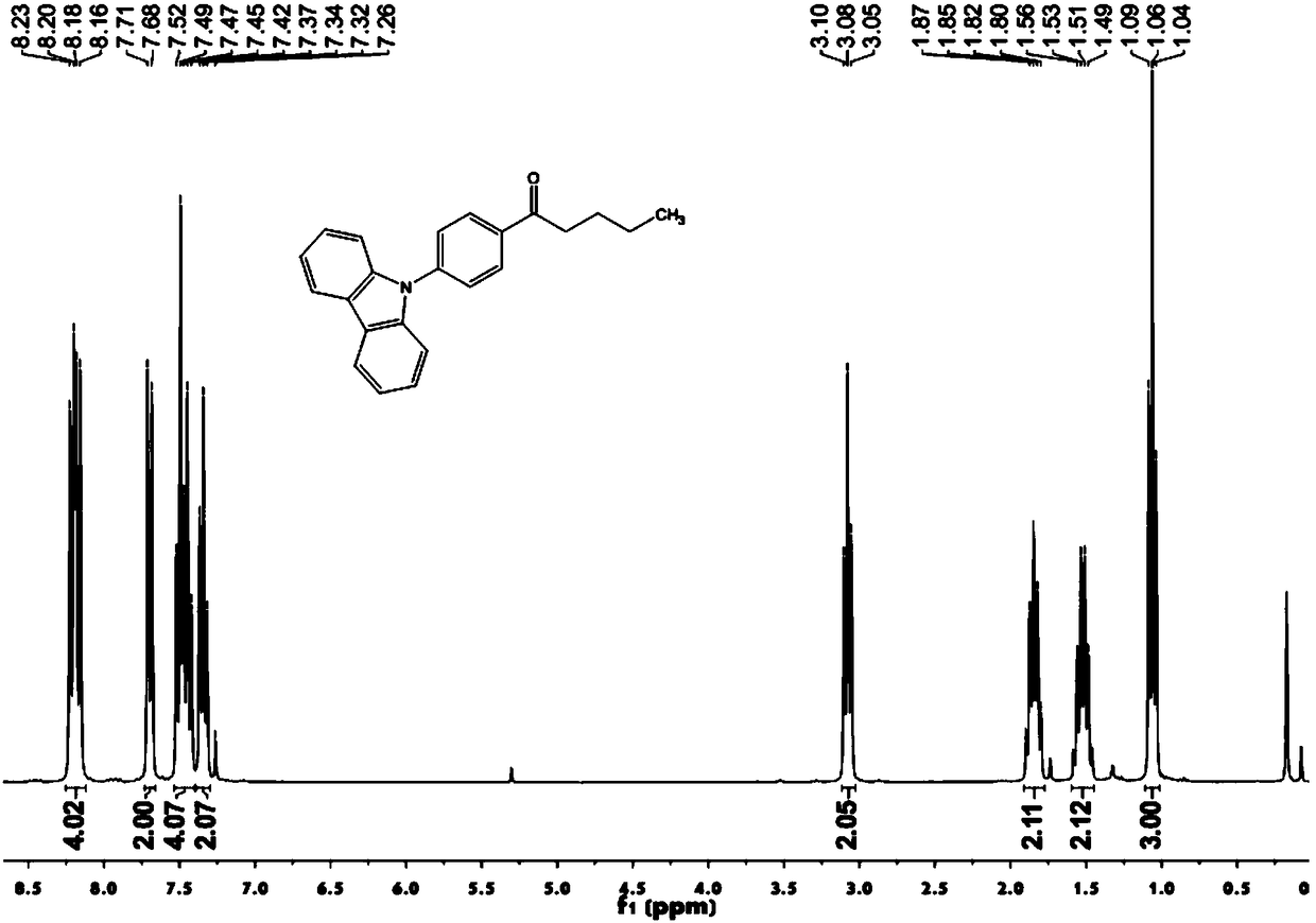
[0048] Embodiment 1: the synthesis of compound 1
[0049]
[0050] Add 2g (0.018mol) of dimethylcarbamoyl chloride and 20ml of tetrahydrofuran solvent to the reaction vessel in turn, deoxygenate the device, pass in nitrogen protection, cool down to the temperature of the reaction solution to -75~-65°C, and slowly add 10ml of 1.6Mn-BuLi / THF solution, control the temperature of the reaction solution at -75~-65°C, after the dropwise addition, continue to maintain this temperature for 0.5-1h. Finally, 6g of compound 1-1 was added dropwise, and the temperature of the reaction solution was controlled at -75~-65°C. After the dropwise addition, the reaction was continued at this temperature for 0.5-1h, and then the reaction solution was moved to room temperature and reacted for 4-6h. Stop responding. Ethyl acetate / deionized water was added for extraction, and the aqueous layer was extracted with ethyl acetate again. The organic layers were combined, dried over anhydrous magnesium ...
Embodiment 2
[0051] Example 2: The following are application examples of the compounds of the present invention.
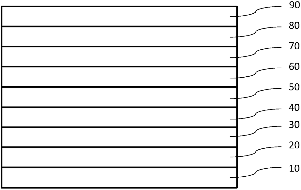
[0052] Device structure such as figure 1 . Device preparation method:
[0053] Firstly, the transparent conductive ITO glass (the glass substrate 10 with the anode 20 ) is cleaned sequentially by detergent solution, deionized water, acetone ultrasonically, isopropanol steam, and then treated with oxygen plasma for 5 minutes.
[0054] Then, 35 nm-thick NPB was vapor-deposited on the ITO as the hole transport layer 30 .
[0055] Then, mCP was evaporated as the electron / exciton blocking layer 40 to a thickness of 5 nm.
[0056] Then, a luminescent layer 50 with a thickness of 20 nm was evaporated, using mCP as the host material, compound 1 of the present invention as the dopant material, and the doping concentration was 3%.
[0057] Then, mCP was vapor-deposited as the exciton blocking layer 60 to a thickness of 10 nm.
[0058] Then, TPBi was vapor-deposited as the electron ...
PUM
| Property | Measurement | Unit |
|---|---|---|
| wavelength | aaaaa | aaaaa |
| wavelength | aaaaa | aaaaa |
Abstract
Description
Claims
Application Information
 - Generate Ideas
- Intellectual Property
- Life Sciences
- Materials
- Tech Scout
- Unparalleled Data Quality
- Higher Quality Content
- 60% Fewer Hallucinations
Browse by: Latest US Patents, China's latest patents, Technical Efficacy Thesaurus, Application Domain, Technology Topic, Popular Technical Reports.
© 2025 PatSnap. All rights reserved.Legal|Privacy policy|Modern Slavery Act Transparency Statement|Sitemap|About US| Contact US: help@patsnap.com