
Silicon-based SERS chip for quantitatively detecting lead ion concentration in actual water sample and preparation method thereof

A quantitative detection, lead ion technology, applied in measurement devices, instruments, material analysis by optical means, etc., can solve the problems of unsatisfactory sensitivity and reproducibility, limited application, etc., to achieve good selectivity and reliability. cyclic effect

Inactive Publication Date: 2016-08-10
SUZHOU UNIV
View PDF6 Cites 8 Cited by
  • Summary
  • Abstract
  • Description
  • Claims
  • Application Information

AI Technical Summary

Problems solved by technology

Although these SERS sensors are feasible, the sensitivity and reproducibility are not satisfactory, thus limiting their application in real water samples

Method used


Image

  • Silicon-based SERS chip for quantitatively detecting lead ion concentration in actual water sample and preparation method thereof
  • Silicon-based SERS chip for quantitatively detecting lead ion concentration in actual water sample and preparation method thereof
  • Silicon-based SERS chip for quantitatively detecting lead ion concentration in actual water sample and preparation method thereof

Examples


Embodiment 1

[0044] Embodiment 1: Preparation of the silicon-based SERS chip of the present invention

[0045] (1) Preparation of silver nanoparticles modified silicon wafers by hydrofluoric acid assisted etching method

[0046] Take 0.5cm 2 3-6 single crystal silicon wafers of large and small sizes were placed in a clean beaker and ultrasonically cleaned with deionized water, acetone, and deionized water for 15 minutes in an ultrasonic instrument, and then 40 mL of concentrated sulfuric acid and hydrogen peroxide (mass concentration: 40 %) mixed solution (volume ratio=3:1) for further cleaning, and then cleaning with deionized water to obtain a clean silicon wafer. Put the cleaned silicon wafer into a hydrofluoric acid solution (mass concentration: 5%) for silicon-hydrogenation reaction, shake slowly for 30 minutes, and obtain a silicon wafer covered with a large number of Si-H bonds on the surface. Put the silicon wafer obtained after the above treatment with the shiny side up, into 20...

Embodiment 2

[0051] Embodiment 2: Preparation of the silicon-based SERS chip of the present invention

[0052] (1) Preparation of silver nanoparticles modified silicon wafers by hydrofluoric acid assisted etching method

[0053] Take 0.5cm 2 3-6 single crystal silicon wafers of large and small sizes were placed in a clean beaker and ultrasonically cleaned with deionized water, acetone, and deionized water for 15 minutes in an ultrasonic instrument, and then 40 mL of concentrated sulfuric acid and hydrogen peroxide (mass concentration: 40 %) mixed solution (volume ratio=3:1) for further cleaning, and then cleaning with deionized water to obtain a clean silicon wafer. Put the cleaned silicon wafer into a hydrofluoric acid solution (mass concentration: 5%) for silicon-hydrogenation reaction, shake slowly for 30 minutes, and obtain a silicon wafer covered with a large number of Si-H bonds on the surface. Put the silicon wafer obtained after the above treatment with the shiny side up, into 20...

Embodiment 3

[0058] Embodiment 3: Preparation of the silicon-based SERS chip of the present invention

[0059] (1) Preparation of silver nanoparticles modified silicon wafers by hydrofluoric acid assisted etching method

[0060] Take 0.5cm 2 3-6 single crystal silicon wafers of large and small sizes were placed in a clean beaker and ultrasonically cleaned with deionized water, acetone, and deionized water for 15 minutes in an ultrasonic instrument, and then 40 mL of concentrated sulfuric acid and hydrogen peroxide (mass concentration: 40 %) mixed solution (volume ratio=3:1) for further cleaning, and then cleaning with deionized water to obtain a clean silicon wafer. Put the cleaned silicon wafer into a hydrofluoric acid solution (mass concentration: 5%) for silicon-hydrogenation reaction, shake slowly for 30 minutes, and obtain a silicon wafer covered with a large number of Si-H bonds on the surface. Put the silicon wafer obtained after the above treatment with the shiny side up, into 20...


PUM

PropertyMeasurementUnit
sizeaaaaaaaaaa
sizeaaaaaaaaaa

Abstract

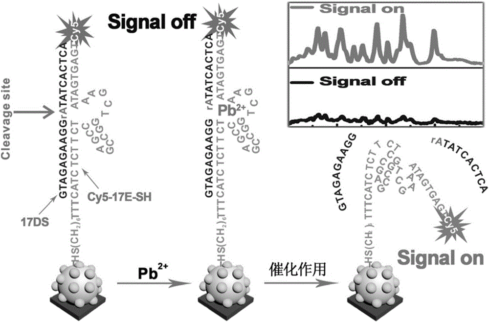
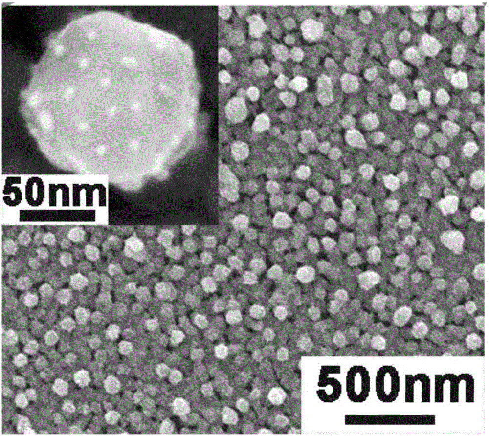
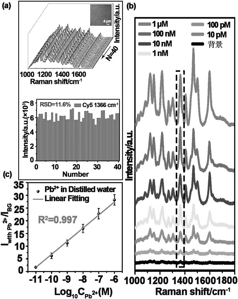
The invention relates to the field of environment monitoring and discloses a silicon-based SERS chip for quantitatively detecting lead ion concentration in an actual water sample and a preparation method thereof. The chip is composed of: a silicon wafer modified with silver nano particles, gold nano particles, nucleotide sequences represented as the SEQ ID No.1, 2, and 4, and a sequence fragment formed by coupling a sulfydryl group to a 5-terminal and coupling a fluorescent dye to a 3-terminal of a nucleotide sequence SEQ ID No.3. In the invention, the surface enhanced Raman scattering silicon-based chip with assistance of polyadenine is employed for detecting the lead ion, wherein the chip is composed of core (silver) and satellite (gold) nano particles, wherein the DNAzyme covalently connected to the chip can be excited specifically by the lead ions, so that the substrate strand is broken into two free DNA segments. The chip can detect a strong SERS signal, and achieves high sensitivity, specificity, repeatability and recyclability.

Description

technical field [0001] The invention relates to the technical field of environmental monitoring, in particular to a silicon-based SERS chip for quantitatively detecting the concentration of lead ions in actual water samples and a preparation method thereof. Background technique [0002] Lead ion is one of the most dangerous heavy metal ions in the environment, and there are many sources such as food, blood, drinking water, industrial wastewater, etc. Studies have found that lead pollution through the food chain and drinking water can cause serious damage to humans, especially children's nervous system, urinary system, and intellectual development (see: Int.J.Hyg.Environ.Health 2008,211,345-351; Annu. Rev. Med. 2004, 55, 209-222). Lead ions are not easy to degrade in the human body, so long-term accumulation and even a small amount of lead ions will affect human health. The U.S. Environmental Protection Agency stipulates that the maximum residual amount of lead ions in drin...

Claims


Application Information

Patent Timeline
Patent Type & Authority Applications(China)
IPC IPC(8): G01N21/65
CPCG01N21/658
Inventor 何耀史宇王后禹
Owner SUZHOU UNIV
Learn More