Photoetching and etching method for preventing shaped wafer surface from etching damage

A surface etching and wafer technology, applied in electrical components, semiconductor/solid-state device manufacturing, circuits, etc., can solve the problems of etching damage, insufficient barrier of advanced patterned film in gate polysilicon area, etc., saving time and cost. cost effect

Active Publication Date: 2016-08-10
SHANGHAI HUALI MICROELECTRONICS CORP
View PDF4 Cites 7 Cited by
  • Summary
  • Abstract
  • Description
  • Claims
  • Application Information

AI Technical Summary

Problems solved by technology

[0005] However, according to this conventional process as shown in the figure: the process of gate polysilicon treatment and then control gate treatment, due to the height difference in the formed peripheral gate polysilicon area, the t...

Method used


Image

  • Photoetching and etching method for preventing shaped wafer surface from etching damage
  • Photoetching and etching method for preventing shaped wafer surface from etching damage
  • Photoetching and etching method for preventing shaped wafer surface from etching damage

Examples


Embodiment Construction

[0033] In order to make the content of the present invention clearer and easier to understand, the content of the present invention will be described in detail below in conjunction with specific embodiments and accompanying drawings.

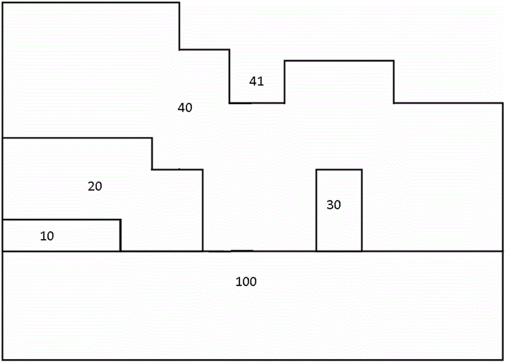
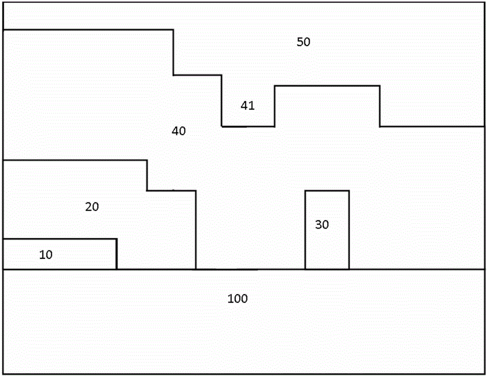
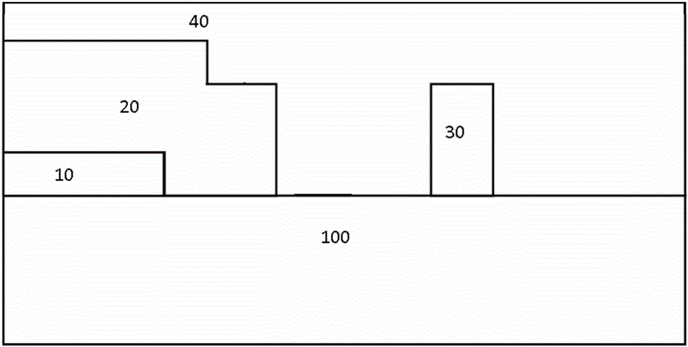
[0034] The invention adopts an innovative high-level patterned thin film planarization process to solve the problem of etching damage that often occurs on the surface of a shaped wafer. In the present invention, the surface topography of the wafer is filled and leveled by the gap filling material, and then the planarization process is carried out to realize the surface planarization of the advanced patterned film, and then the photolithography and etching process are carried out to solve the problem of the surface pattern of the wafer. Etching damage due to height difference.

[0035] Specific preferred embodiments of the present invention will be described below in conjunction with the accompanying drawings.

[0036] Figure 1 to Figure 6 Eac...


PUM


Abstract

The invention provides a photoetching and etching method for preventing shaped wafer surface from etching damage. The method comprises following steps of forming a floating gate layer and a storage unit control gate layer on a substrate in a storage unit region; forming a gate polysilicon layer on the substrate in a periphery region; depositing advanced patterned film on the substrate; forming a gap filling material layer on the advanced patterned film, thus filling the concave and convex parts of the advanced patterned film; carrying out shape planarization on the advanced patterned film by using a planarization back processing technology; depositing anti-reflection coating film; coating photoresist; forming photoresist patterns; and executing etching processing by using the photoresist patterns, thus etching the floating gate layer and the storage unit control gate layer.

Description

technical field [0001] The invention relates to the field of semiconductor manufacturing, more specifically, the invention relates to a photolithographic etching method for preventing etching damage on the surface of a wafer with topography. Background technique [0002] In the flash memory process, due to the requirements for the formation of the flash memory area and the peripheral area, the polysilicon process of the control gate and the peripheral gate of the memory cell is usually carried out in two steps. [0003] In the case of large design specifications and line widths, traditional photolithography processes such as KrF can use thick photoresist solutions to ensure sufficient photoresist barrier layers. [0004] However, when the line width is lower than a certain specification, an immersion lithography solution is required. The conventional process is: first fill with an advanced patterned film, then fill with an anti-reflective coating (BARC), and then perform a l...

Claims


Application Information

Patent Timeline
IPC IPC(8): H01L21/311
CPCH01L21/311
Inventor 殷冠华陈昊瑜顾珍
Owner SHANGHAI HUALI MICROELECTRONICS CORP
Why Eureka
Try Eureka