High-efficiency nano-structure light emitting diode (LED) and design and fabrication methods thereof

A nano-structured, high-efficiency technology, applied in electrical components, circuits, semiconductor devices, etc., can solve the problem of difficulty in improving light extraction efficiency, and achieve the effect of improving light extraction efficiency and reducing reflectivity

Inactive Publication Date: 2016-08-10
GUANGDONG POLYTECHNIC NORMAL UNIV
View PDF4 Cites 11 Cited by
  • Summary
  • Abstract
  • Description
  • Claims
  • Application Information

AI Technical Summary

Problems solved by technology

[0003] However, it is generally difficult to increase the light extraction efficiency of the above-mentioned technologies by more than

Method used


Image

  • High-efficiency nano-structure light emitting diode (LED) and design and fabrication methods thereof
  • High-efficiency nano-structure light emitting diode (LED) and design and fabrication methods thereof
  • High-efficiency nano-structure light emitting diode (LED) and design and fabrication methods thereof

Examples


Example Embodiment

[0054] Example 1

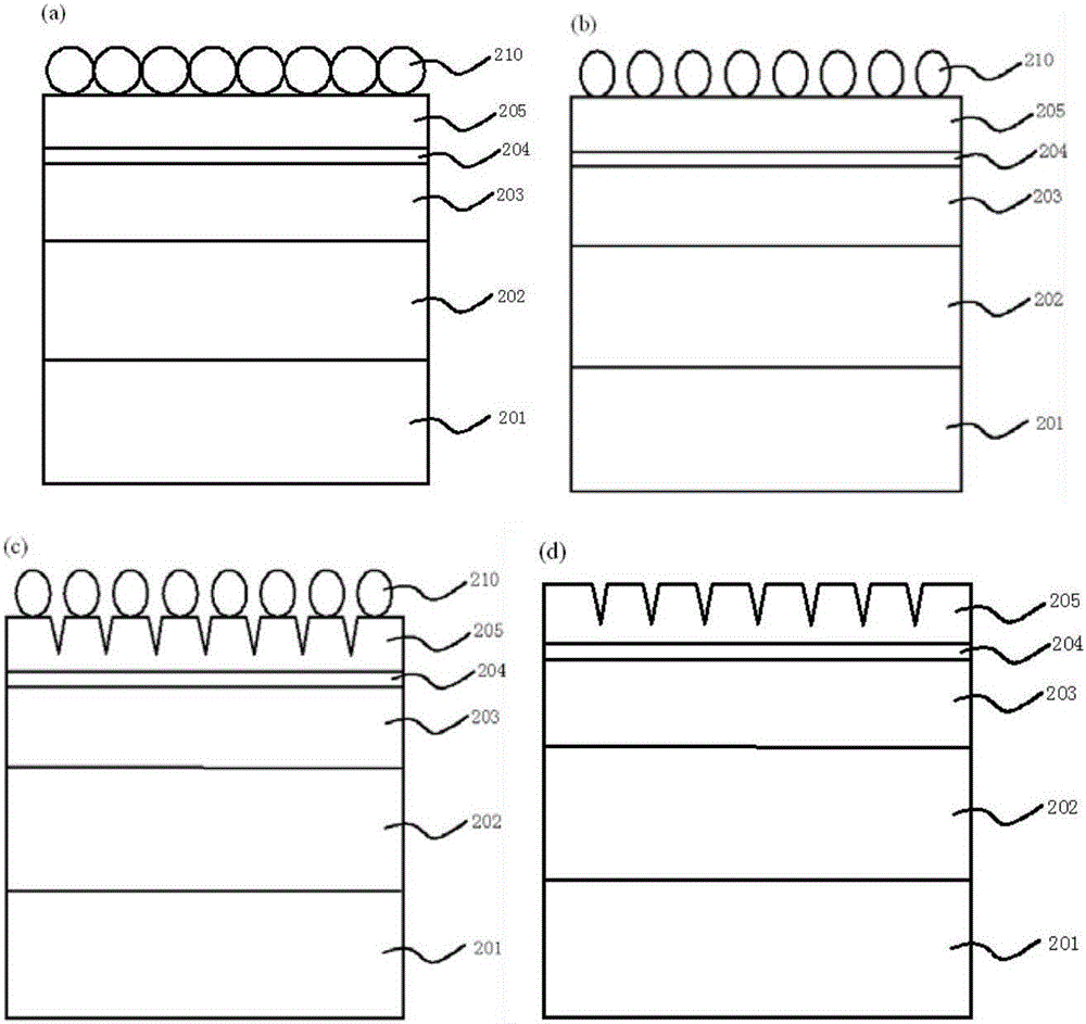
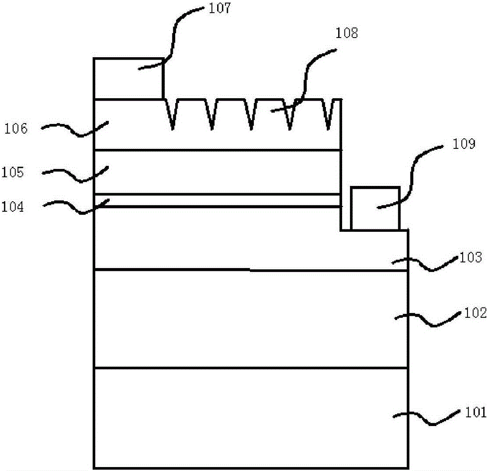
[0055] Such as Figure 1-Figure 16 As shown, a high-efficiency nanostructured LED provided by the present invention includes a substrate 101, an undoped GaN layer 102 formed on the substrate 101, and an n-doped GaN layer 103 formed on the undoped GaN layer 102. , The multiple quantum well layer 104 formed on the n-doped GaN layer 103, the p-doped GaN layer 105 formed on the multiple quantum well layer 104, the ITO layer 106 formed on the p-doped GaN layer 105, formed on ITO The nanostructures on the layer 108 are nano-pillar arrays 108 distributed on the ITO.

[0056] Among them, the substrate 101 is a sapphire substrate with poor conductivity to prevent short circuit of the electrodes. The materials of the non-doped GaN layer 102, the n-doped GaN layer 103, the multi-quantum well layer 104, and the p-doped GaN layer 105 are set according to the performance of the chip, which are common knowledge of those skilled in the art, and will not be repeated here.

[005...


PUM

PropertyMeasurementUnit
Heightaaaaaaaaaa
Diameteraaaaaaaaaa
Diameteraaaaaaaaaa

Abstract

The invention discloses a high-efficiency nano-structure light emitting diode (LED) and design and fabrication methods thereof. The design method comprises the following steps of 1) designing a period of a nanopillar array by a Bragg diffraction theory; 2) designing the diameter and the height of a nanopillar by an effective refractive index and enhanced thin film transmittance; and 3) fabricating a nanopillar array structure by nanosphere mark etching or other nanometer technologies. The high-efficiency nano-structure LED is ingenious in design and can be produced at a large scale, and a planar-structure LED chip with high efficiency is fabricated by optimally designing the nanopillar structure. With the design and fabrication methods of the high-efficiency LED, disclosed by the invention, the nanopillar array structure is designed on an ITO layer of a transparent electrode of the LED, and the high-efficiency planar-structure LED is fabricated.

Description

technical field [0001] The invention provides a high-efficiency nanostructure LED and a design and preparation method thereof. Background technique [0002] As an alternative to traditional lamps, Light emitting diode (LED) lighting has a bright future and is known as a new generation of light sources (Laser & Photon Rev, 2009, 3:262). The LED light source directly converts electrical energy into light energy, and the energy conversion efficiency is quite high. In theory, it only needs 10% of the energy consumption of incandescent lamps or 50% of the energy consumption of fluorescent lamps. However, the luminous efficiency of LEDs is still low at present, and this shortcoming makes the performance of current LED devices unsatisfactory. The lower light extraction efficiency is due to the large refractive index difference between the semiconductor material and the surrounding air (Appl Phys Lett., 2006, 88:083121). According to Snell's law, most photons will be totally reflec...

Claims


Application Information

Patent Timeline
IPC IPC(8): H01L33/00H01L33/58H01L33/60
CPCH01L33/60H01L33/0075H01L33/58H01L2933/0058
Inventor 陈湛旭何影记万巍陈泳竹陈耿炎
Owner GUANGDONG POLYTECHNIC NORMAL UNIV
Why Eureka
Try Eureka