n-type Cu2Sn3S7-based medium-high temperature thermoelectric semiconductor and mechanical alloying preparation technique thereof

A thermoelectric semiconductor and mechanical alloying technology, applied in the field of new materials, can solve the problems of complex preparation process, insufficient performance, and high difficulty of thermoelectric semiconductors, and achieve the effects of rich content, long life and reliable operation

Inactive Publication Date: 2016-09-28
NINGBO UNIVERSITY OF TECHNOLOGY
View PDF4 Cites 3 Cited by
  • Summary
  • Abstract
  • Description
  • Claims
  • Application Information

AI Technical Summary

Problems solved by technology

[0004] To overcome Cu 2 sn 3 S 7 The preparation process of thermoelectric semiconductors is complicated, difficult and has insufficient performance. The present invention aims to provide the field with a higher performance n-type Cu 2 sn 3 S 7 High temperature thermoelectric semiconductor in base and its mechanical alloying preparation process

Method used


Image

  • n-type Cu2Sn3S7-based medium-high temperature thermoelectric semiconductor and mechanical alloying preparation technique thereof
  • n-type Cu2Sn3S7-based medium-high temperature thermoelectric semiconductor and mechanical alloying preparation technique thereof

Examples


Embodiment 1

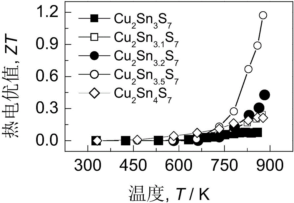
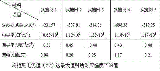
[0013] According to the chemical formula Cu 2 sn 3 S 7 Weigh Cu, Sn, and S three-element particles with a purity greater than 99.999wt.%, and then place them directly in a vacuum ball mill jar for ball milling for 2 hours. The ball-milled powder was placed in a vacuum quartz tube and heated to 700°C for 48 hours for annealing. The annealed powder is formed by spark plasma sintering in a short period of time. The sintering time is 4 minutes, the sintering temperature is 700°C, and the sintering pressure is 60MPa. Cu 2 sn 3 S 7 thermoelectric semiconductors.

Embodiment 2

[0015] According to the chemical formula Cu 2 sn 3.1 S 7 Weigh Cu, Sn, and S three-element particles with a purity greater than 99.999wt.%, and then place them directly in a vacuum ball mill jar for ball milling for 2 hours. The ball-milled powder was placed in a vacuum quartz tube and heated to 700°C for 48 hours for annealing. The annealed powder is formed by spark plasma sintering in a short period of time. The sintering time is 4 minutes, the sintering temperature is 700°C, and the sintering pressure is 60MPa. Cu 2 sn 3.1 S 7 thermoelectric semiconductors.

Embodiment 3

[0017] According to the chemical formula Cu 2 sn 3.2 S 7 Weigh Cu, Sn, and S three-element particles with a purity greater than 99.999wt.%, and then place them directly in a vacuum ball mill jar for ball milling for 2 hours. The ball-milled powder was placed in a vacuum quartz tube and heated to 700°C for 48 hours for annealing. The annealed powder is formed by spark plasma sintering in a short period of time. The sintering time is 4 minutes, the sintering temperature is 700°C, and the sintering pressure is 60MPa. Cu 2 sn 3.2 S 7 thermoelectric semiconductors.


PUM

PropertyMeasurementUnit
electrical conductivityaaaaaaaaaa
thermal conductanceaaaaaaaaaa

Abstract

The invention relates to an n-type Cu2Sn3S7-based medium-high temperature thermoelectric semiconductor and a mechanical alloying preparation technique thereof. The key point of the design of the n-type Cu2Sn3S7-based medium-high temperature thermoelectric semiconductor lies in that the Sn content is increased on the basis of the compositions of Cu2Sn3S7, and the chemical formula of Cu2Sn3.5S7 is formed. The mechanical alloying preparation technique of the n-type Cu2Sn3S7-based medium-high temperature thermoelectric semiconductor comprises the steps that the corresponding quantity of Cu, the corresponding quantity of Sn and the corresponding quantity of S are weighed according to the chemical formula and placed in a vacuum ball milling tank to be subjected to ball milling for two hours; annealing is conducted for 48 hours in a vacuum tube at the temperature of 700 DEG C after ball milling; then powder is taken out and subjected to discharge plasma spark sintering in a short time of four minutes for formation; and the highest sintering temperature is 700 DEG C, the sintering pressure is 60 MPa, and a Cu2Sn3.5S7 thermoelectric semiconductor is prepared. The Seebeck coefficient a of the thermoelectric semiconductor at the temperature of 877 K is -698.38 (<mu>V/K), the electric conductivity s is 1.18'10<3>W<-1>.m<-1>, the heat conductivity k is 0.43(W.K<-1>.m<-1>), and the maximum thermoelectric optimum value ZT is 1.17. The n-type Cu2Sn3S7-based medium-high temperature thermoelectric semiconductor has the advantages that pollution and noise are avoided, the semiconductor can be used for manufacturing medium-high temperature power generation components, operation is reliable, the service life is long, and the preparation technique is simple.

Description

technical field [0001] The invention relates to the field of new materials, which is a key component material for medium temperature power generation that directly converts heat energy and electric energy, and is an n-type Cu 2 sn 3 S 7 Base medium high temperature thermoelectric semiconductor and its preparation process. Background technique [0002] Thermoelectric semiconductor material is a new type of semiconductor functional material that realizes direct mutual conversion of electric energy and thermal energy through the movement of carriers, including electrons or holes. Power generation and refrigeration devices made of thermoelectric materials have the advantages of small size, no pollution, no noise, no wear, good reliability, and long life. In the civilian field, the potential application range: household refrigerators, freezers, superconducting electronic device cooling and waste heat power generation, waste heat utilization power supply, and small power supply...

Claims


Application Information

Patent Timeline
Patent Type & Authority Applications(China)
IPC IPC(8): C22C29/00C22C1/05C22C1/10
CPCC22C1/05C22C1/1084C22C29/00
Inventor 崔教林
Owner NINGBO UNIVERSITY OF TECHNOLOGY
Why Eureka
Try Eureka