Liquid crystal display panel and making method thereof

A liquid crystal display panel and manufacturing method technology, applied in optics, instruments, nonlinear optics, etc., can solve the problems of expensive PI materials, weak ability to anchor liquid crystal molecules, dust particles, static electricity residues, etc., to simplify the liquid crystal alignment process. , Improve the effect of liquid crystal alignment and good electrical conductivity

Active Publication Date: 2016-09-28
SHENZHEN CHINA STAR OPTOELECTRONICS TECH CO LTD
View PDF7 Cites 17 Cited by
  • Summary
  • Abstract
  • Description
  • Claims
  • Application Information

AI Technical Summary

Problems solved by technology

[0006] In addition, on the CF substrate and the TFT substrate, there is also a thin film respectively, whose main function is to arrange the liquid crystal molecules in a certain direction. We call it an alignment film. The material of the alignment film mainly includes rubbing alignment type PI (polymer imide) materials and photo-aligned PI materials, however, no matter which PI material has its own shortcomings, first of all, frictional alignment is likely to cause problems such as dust particles, static electricity residue, and brush marks, thereby reducing the process yield. Although alignment materials can avoid these problems, due to limited material properties, poor heat resistance and aging resistance, and weak ability to anchor liquid crystal molecules, thus affecting the quality of the panel; secondly, the PI material itself has high polarity. High water absorption, easy to deteriorate during storage and transportation, resulting in uneven alignment, and PI materials are expensive, and the process of film formation on TFT-LCD is also relatively complicated, resulting in increased panel costs

Method used


Image

  • Liquid crystal display panel and making method thereof
  • Liquid crystal display panel and making method thereof
  • Liquid crystal display panel and making method thereof

Examples


Embodiment Construction

[0064] In order to further illustrate the technical means adopted by the present invention and its effects, the following describes in detail in conjunction with preferred embodiments of the present invention and accompanying drawings.

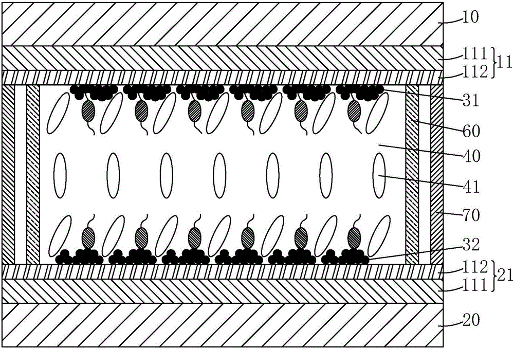
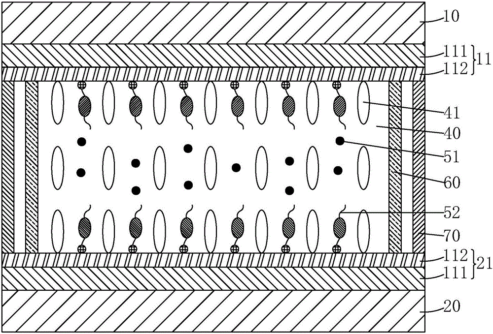
[0065] see figure 1 , the present invention firstly provides a liquid crystal display panel, comprising a CF substrate 10 and a TFT substrate 20 disposed opposite to each other, a common electrode 11 and a pixel electrode 21 respectively arranged on opposite sides of the CF substrate 10 and the TFT substrate 20, and respectively arranged on The first polymer layer 31 and the second polymer layer 32 on the opposite side of the common electrode 11 and the pixel electrode 21, and the liquid crystal layer arranged between the first polymer layer 31 and the second polymer layer 32 40. The liquid crystal layer 40 includes liquid crystal molecules 41;

[0066] Both the common electrode 11 and the pixel electrode 21 include a graphene layer 111;

[...


PUM


Abstract

The invention provides a liquid crystal display panel and a making method thereof. Graphene is adopted to replace indium tin oxide to make common electrodes and pixel electrodes, by means of the advantages of graphene that the transparency is high, the conductivity property is good, the flexibility is high and the production cost is low, the display performance of the liquid crystal display penal is improved, and the production cost of the liquid crystal display panel is reduced; a vertical alignment agent and polymeric monomers are utilized for conducting alignment on liquid crystal molecules, alignment film is omitted, and the liquid crystal alignment process is simplified; further, a graphene oxide layer is arranged on the surface of a graphene layer, the capacity that the vertical alignment agent anchors a substrate can be improved, and the liquid crystal alignment effect is improved.

Description

technical field [0001] The invention relates to the field of display technology, in particular to a liquid crystal display panel and a manufacturing method thereof. Background technique [0002] With the development of display technology, liquid crystal displays (Liquid Crystal Display, LCD) and other flat display devices are widely used in mobile phones, televisions, personal Various consumer electronic products such as digital assistants, digital cameras, notebook computers, and desktop computers have become the mainstream of display devices. [0003] Most of the liquid crystal display devices currently on the market are backlight liquid crystal displays, which include a liquid crystal display panel and a backlight module. The working principle of the liquid crystal display panel is to place liquid crystal molecules between two parallel glass substrates. There are many vertical and horizontal small wires between the two glass substrates. The direction of the liquid crysta...

Claims


Application Information

Patent Timeline
Patent Type & Authority Applications(China)
IPC IPC(8): G02F1/1343G02F1/1337
CPCG02F1/133711G02F1/13439G02F1/133715
Inventor 兰松
Owner SHENZHEN CHINA STAR OPTOELECTRONICS TECH CO LTD
Why Eureka
Try Eureka