Nonvolatile memory manufacturing method thereof

A non-volatile, memory technology, used in semiconductor/solid-state device manufacturing, electrical solid-state devices, semiconductor devices, etc., can solve the problem of shortening the length of the tunnel oxide layer channel, reducing the reliability of memory elements, and affecting the electrical performance of memory cells. and other problems, to achieve the effect of increasing the speed, reducing the erasing voltage, and reducing the operating voltage

Active Publication Date: 2016-10-05
IOTMEMORY TECH +1
View PDF3 Cites 8 Cited by
  • Summary
  • Abstract
  • Description
  • Claims
  • Application Information

AI Technical Summary

Problems solved by technology

However, the shortening of the gate length will shorten the channel length (Channel Length) under the tunnel oxide layer, which will easily cause abnormal electrical penetration (Punch Through) between the drain and the source, which will seriously affect the memory cell. electrical performance
Moreover, when programming and / or erasing memory cells, electrons repeatedly pass through the tunnel oxide layer, which will wear out the tunnel oxide layer, resulting in reduced reliability of the memory element.

Method used


Image

  • Nonvolatile memory manufacturing method thereof
  • Nonvolatile memory manufacturing method thereof
  • Nonvolatile memory manufacturing method thereof

Examples


Embodiment Construction

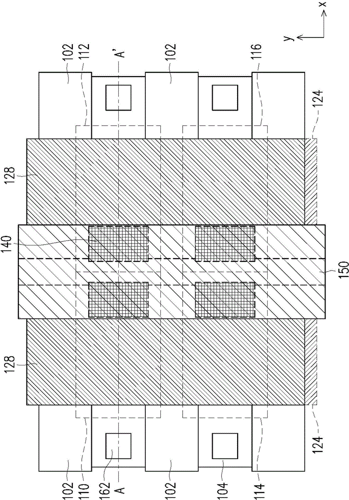
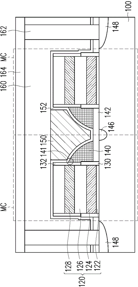
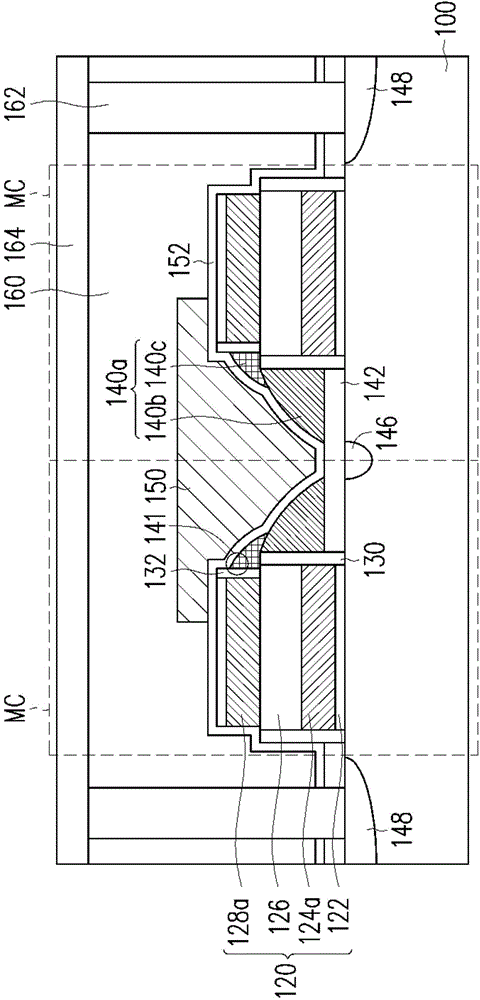
[0072] Figure 1A It is a top view of a non-volatile memory shown in an embodiment of the present invention. Figure 1B It is a schematic cross-sectional view of a non-volatile memory shown in an embodiment of the present invention. Figure 1B shown as along the Figure 1A Sectional view of line A-A' in the middle. Figure 1C It is a schematic cross-sectional view of a non-volatile memory shown in another embodiment of the present invention.

[0073] Please refer to Figure 1A and Figure 1B , the nonvolatile memory includes a plurality of memory cells MC. These memory cells MC are arranged in a row / column array.

[0074] The nonvolatile memory is disposed on the substrate 100 . For example, a plurality of isolation structures 102 arranged regularly are disposed in the substrate 100 to define an active region 104 having a lattice shape. The isolation structure 102 is, for example, a shallow trench isolation structure.

[0075] Each memory cell MC includes a stack structu...


PUM


Abstract

The invention provides a nonvolatile memory, which has a storage unit. The memory unit has a stack structure, a floating gate, a tunnel dielectric layer, an erase gate dielectric layer, an auxiliary gate dielectric layer, a source region, a drain region, a control gate and an inter-gate dielectric layer. The stack structure has a gate dielectric layer, an auxiliary gate, an insulating layer and an erasing gate arranged in sequence. The floating gate is disposed on the sidewall of the first side of the stack structure. The tunneling dielectric layer is disposed under the floating gate. The erasure gate dielectric layer is disposed between the erasure gate and the floating gate. The auxiliary gate dielectric layer is disposed between the auxiliary gate and the floating gate. The source region and the drain region are respectively disposed on two sides of the stack structure and the floating gate. The control gate is disposed on the source region and the floating gate. The inter-gate dielectric layer is disposed between the control gate and the floating gate.

Description

technical field [0001] The present invention relates to a semiconductor element and its manufacturing method, and in particular to a non-volatile memory and its manufacturing method. Background technique [0002] Non-volatile memory has been widely used in personal computers and electronic devices due to its advantages that data can be stored, read, and erased multiple times, and the stored data will not disappear after power failure. [0003] A typical non-volatile memory is designed to have a stacked gate (Stack-Gate) structure, which includes a tunnel oxide layer, a floating gate (Floating gate), and an inter-gate dielectric that are sequentially arranged on the substrate. layer and control gate (Control Gate). When programming or erasing the flash memory device, an appropriate voltage is applied to the source region, the drain region and the control gate respectively, so that electrons are injected into the polysilicon floating gate, or electrons are transferred from th...

Claims


Application Information

Patent Timeline
Patent Type & Authority Applications(China)
IPC IPC(8): H01L27/115H01L21/8247
Inventor 郑育明
Owner IOTMEMORY TECH
Why Eureka
Try Eureka