Tunneling Field Effect Transistor and Method of Forming the Same

A tunneling field effect and transistor technology, which is applied in the manufacture of diodes, semiconductor devices, semiconductor/solid-state devices, etc., can solve the problems of leakage current destroying sub-threshold swing, difficult to realize narrow tunnel junction, and difficult to turn off devices , to achieve the effect of improving sub-threshold characteristics, reducing leakage current, and increasing conduction current

Active Publication Date: 2019-12-13
INST OF MICROELECTRONICS CHINESE ACAD OF SCI
View PDF4 Cites 0 Cited by
  • Summary
  • Abstract
  • Description
  • Claims
  • Application Information

AI Technical Summary

Problems solved by technology

However, in order to reduce the sub-threshold swing and increase the conduction current, the tunneling junction needs to be as narrow as possible. However, the tunneling field effect transistor with the existing structure will always cause the diffusion distribution of impurities during the injection and heat treatment process, and it is difficult to achieve a narrow tunneling junction. tunneling junction
[0005] In addition, in conventional tunneling field effect transistors, the source and drain regions are highly doped, and the doping will inevitably introduce defects, and the leakage current associated with these defects will destroy the reduction of the subthreshold swing.
Moreover, conventional tunneling field effect transistors have bipolar characteristics that can be turned on at both positive and negative gate voltages, making it difficult to completely turn off the device

Method used


Image

  • Tunneling Field Effect Transistor and Method of Forming the Same
  • Tunneling Field Effect Transistor and Method of Forming the Same
  • Tunneling Field Effect Transistor and Method of Forming the Same

Examples


Embodiment 1

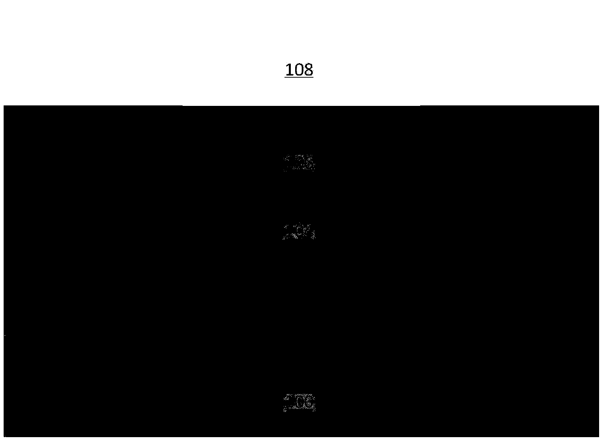
[0079] First, in step S101, the substrate 100 is provided, refer to figure 1 shown.

[0080] In this embodiment, a silicon substrate is used as the substrate, and the silicon substrate may be, for example, a bulk silicon substrate, an SOI (silicon-on-insulator) substrate or other stacked substrates. In other embodiments, other substrates may also be used, and the substrate functions as a support and an epitaxial base.

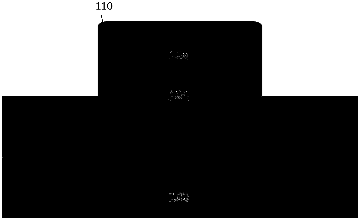
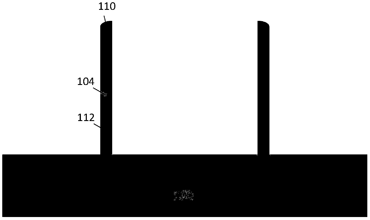
[0081] Next, in step S102, epitaxial fins 112 are formed on the substrate, refer to image 3 shown.

[0082] In this embodiment, in order to obtain small-sized fins, for example, the width of the fins 112 is controlled to be about 10 nm or narrower, after epitaxy of a material layer on the substrate, the fins can be formed by the method of transferring the sidewall pattern.

[0083] Specifically, first, a first epitaxial layer 102 is formed on the silicon substrate 100 by an epitaxial process, and the first epitaxial layer can be an epitaxial III-V semicond...

Embodiment 2

[0106] First, in step S201, a substrate 200 is provided, refer to Figure 15 shown.

[0107] In this embodiment, a silicon substrate is used as the substrate, and the silicon substrate may be, for example, a bulk silicon substrate, an SOI (silicon-on-insulator) substrate or other stacked substrates. In other embodiments, other substrates may also be used, and the substrate functions as a support and an epitaxial base.

[0108] Next, in step S202, a first epitaxial layer 202 is formed on the silicon substrate by an epitaxial process, and the first epitaxial layer may be an epitaxial III-V semiconductor material, such as InAs, InSb, SiGe, InGaAs, SiGeSn And so on, other semiconductor materials such as Ge, GeSi, etc. can also be used. These epitaxial materials have higher tunneling probability than silicon substrates. In this way, the tunneling current of the channel can be further improved, and the performance of the device can be improved.

[0109] Then, in step S203, source ...


PUM


Abstract

The invention provides a tunneling field effect transistor which comprises a substrate with the formation of a fin with an epitaxial, first and second grids formed on opposite side walls of the fin, a first gate dielectric layer which is formed between the first grid and the side wall of the fin and the bottom surface of the first grid, a second gate dielectric layer which is formed between the second grid and the side wall of the fin and the bottom surface of the second grid, and source and drain regions which are formed at one side of the first grid and one side of the second grid. According to the tunneling field effect transistor with the structure, through controlling the width of the fin, a narrow tunneling junction without the limitation of impurity injection diffusion is realized, the tunneling current is increased, and the conduction current is further raised through increasing an effective tunneling area.

Description

technical field [0001] The present invention relates to the field of semiconductor devices, in particular to a tunneling field effect transistor and a method for forming the same. Background technique [0002] With the continuous reduction of device size, the number of devices per unit area of ​​the chip is increasing, and how to reduce power consumption has become an increasingly prominent problem. [0003] The structure of a conventional tunneling field effect transistor (conventional-TFET) mainly includes a substrate (channel), a gate dielectric layer, a gate, and source / drain regions on both sides of the gate. It mainly works based on the quantum tunneling effect. Taking the P-type tunneling field effect transistor as an example, when a negative voltage is applied to the gate, the potential of the channel region increases, and quantum tunneling occurs from the source region to the channel region. Drain area outflow. [0004] For conventional tunneling field effect tran...

Claims


Application Information

Patent Timeline
Patent Type & Authority Patents(China)
IPC IPC(8): H01L29/739H01L29/423H01L29/10H01L21/331
CPCH01L29/1033H01L29/42356H01L29/66356H01L29/7391
Inventor 朱正勇朱慧珑许淼
Owner INST OF MICROELECTRONICS CHINESE ACAD OF SCI
Why Eureka
Try Eureka