
Electromagnetic shielding film and preparation method thereof

A technology of electromagnetic shielding film and release film, applied in chemical instruments and methods, conductive coatings, lamination, etc., can solve the problems of expensive equipment, large production space, large production cost, etc., to reduce production space and production efficiency. High and low cost effect

Inactive Publication Date: 2016-10-12
胡银坤
View PDF9 Cites 10 Cited by
  • Summary
  • Abstract
  • Description
  • Claims
  • Application Information

AI Technical Summary

Problems solved by technology

Among them, the metal layer is basically realized by evaporation or magnetron sputtering at present. These equipment are relatively expensive and need to occupy a larger production space, which leads to greater production costs for enterprises.

Method used


Image

  • Electromagnetic shielding film and preparation method thereof

Examples


Embodiment 1

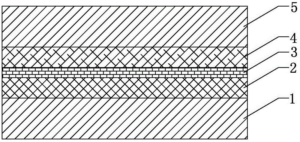
[0032] An electromagnetic shielding film, comprising a carrier film 1, an insulating layer 2, a metal layer 3, a conductive adhesive layer 4 and a release film 5 arranged sequentially from bottom to top, the lower surface and the upper surface of the insulating layer 2 are respectively connected to the carrier film 1 The upper surface of the conductive adhesive layer 4 is attached to the lower surface of the metal layer 3, and the lower surface and the upper surface of the conductive adhesive layer 4 are respectively attached to the upper surface of the metal layer 3 and the lower surface of the release film 5.

[0033] The carrier film 1 is a PET film; the release film 5 is a PET release film 5 with a release force of 5 gf; the thickness of the carrier film 1 is 20 μm; the thickness of the insulating layer 2 is 2 μm; The thickness of the metal layer 3 is 0.2 μm; the thickness of the conductive adhesive layer 4 is 7 μm; the thickness of the release film 5 is 20 μm.

[0034] Th...

Embodiment 2

[0047] The difference between this embodiment and the above-mentioned embodiment 1 is:

[0048] The release film 5 is a PE release film 5 with a release force of 6 gf; the thickness of the carrier film 1 is 40 μm; the thickness of the insulating layer 2 is 4 μm; the thickness of the metal layer 3 is 0.5 μm; The thickness of the conductive adhesive layer 4 is 9 μm; the thickness of the release film 5 is 40 μm.

[0049] The insulating layer 2 is prepared by coating an insulating paint, and the insulating paint is composed of the following raw materials in parts by weight: 100 parts of resin and 2 parts of light-absorbing material.

[0050] The resin is epoxy resin.

[0051] The light-absorbing material is graphite, and the particle size of the light-absorbing material is 1 μm.

[0052] The metal layer 3 is prepared by coating copper ink, and the copper ink is a copper chelate obtained by reacting copper nitrate and ammonium carbamate compounds.

[0053] The conductive adhesiv...

Embodiment 3

[0057] The difference between this embodiment and the above-mentioned embodiment 1 is:

[0058]The release film 5 is an OPP release film 5 with a release force of 8 gf; the thickness of the carrier film 1 is 60 μm; the thickness of the insulating layer 2 is 6 μm; the thickness of the metal layer 3 is 0.8 μm; The thickness of the conductive adhesive layer 4 is 11 μm; the thickness of the release film 5 is 60 μm.

[0059] The insulating layer 2 is prepared by coating an insulating paint, and the insulating paint is composed of the following raw materials in parts by weight: 100 parts of resin and 3 parts of light-absorbing material.

[0060] The resin is polyurethane resin.

[0061] The light-absorbing material is iron oxide black, and the particle size of the light-absorbing material is 0.5 μm.

[0062] The metal layer 3 is prepared by coating copper ink, and the copper ink is a copper chelate obtained by reacting copper nitrate and ammonium carbamate compounds.

[0063] The...


PUM

PropertyMeasurementUnit
thicknessaaaaaaaaaa
thicknessaaaaaaaaaa
thicknessaaaaaaaaaa

Abstract

The invention relates to the technical field of shielding films, in particular to an electromagnetic shielding film and a preparation method thereof, comprising a carrier film, an insulating layer, a metal layer, a conductive adhesive layer and a release film arranged sequentially from bottom to top, and the lower surface of the insulating layer and the upper surface are attached to the upper surface of the carrier film and the lower surface of the metal layer respectively, and the lower surface and the upper surface of the conductive adhesive layer are respectively attached to the upper surface of the metal layer and the lower surface of the release film. The electromagnetic shielding film of the invention has the advantages of simple structure, good electromagnetic shielding effect and low cost. Compared with vacuum coating and measurement and control sputtering, the preparation method of the present invention has high production efficiency, can dispense with coating-related equipment, reduces production space, and saves input and production costs.

Description

technical field [0001] The invention relates to the technical field of shielding films, in particular to an electromagnetic shielding film and a preparation method thereof. Background technique [0002] In recent years, electronic equipment such as PCs, mobile phones, and digital equipment has shown a trend of miniaturization and light weight. The rapid popularization of electronic equipment has also attracted the influence of electromagnetic waves in work units or families. With the development of the electronic industry, the impact of electromagnetic interference The threat is growing. [0003] The existing electromagnetic wave shielding film is composed of an insulating layer, a metal layer and a conductive adhesive layer. Among them, the metal layer is basically realized by evaporation or magnetron sputtering at present. These devices are relatively expensive and need to occupy a larger production space, which leads to greater production costs for enterprises. Content...

Claims


Application Information

Patent Timeline
Patent Type & Authority Applications(China)
IPC IPC(8): B32B27/36B32B27/08B32B7/06B32B33/00B32B37/10C09D5/25C09D5/24C09D133/00C09D7/12C09D163/00C09D175/04C09D167/00
CPCB32B27/36B32B7/06B32B27/08B32B33/00B32B37/10B32B2255/10B32B2255/26C08K3/04C08K3/08C08K5/24C08K2003/0806C08K2003/085C08K2003/0856C08K2003/0862C08K2201/001C08L2205/03C08L2205/035C09D7/61C09D133/00C09D163/00C09D167/00C09D175/04
Inventor 胡银坤
Owner 胡银坤
Learn More