A cmos integrated circuit terahertz detector applied in the field of terahertz skin imaging

A skin imaging, integrated circuit technology, applied in applications, sensors, electrical components, etc., can solve problems such as the impact of simulation accuracy

Inactive Publication Date: 2019-04-05
FUDAN UNIV
View PDF6 Cites 0 Cited by
  • Summary
  • Abstract
  • Description
  • Claims
  • Application Information

AI Technical Summary

Problems solved by technology

If necessary, it is still necessary to establish a separate model for the core device / structure to avoid the impact on the simulation accuracy of these devices / structures due to scaling law extraction errors after the scaling model is established

Method used


Image

  • A cmos integrated circuit terahertz detector applied in the field of terahertz skin imaging
  • A cmos integrated circuit terahertz detector applied in the field of terahertz skin imaging
  • A cmos integrated circuit terahertz detector applied in the field of terahertz skin imaging

Examples


Embodiment Construction

[0016] The invented CMOS integrated circuit terahertz detector applied in the field of terahertz skin imaging will be further described below with reference to the accompanying drawings.

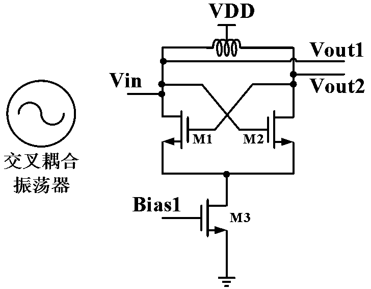
[0017] The circuit structure of the present invention is as attached Figure 4 As shown, it is divided into two modules 101 and 102, wherein module 101 is a circuit for receiving terahertz signals, the source of the NMOS transistor is grounded, the gate is connected to the antenna, the drain is connected to one end of the inductor, and the other end of the inductor is connected to the power supply VDD. The terahertz signal received by the antenna is injected into the low-noise amplifier through AC-coupling of the DC-blocking capacitor. The gate bias voltage of the low-noise amplifier can be adjusted. The drain generates harmonic injection into the module 102 .

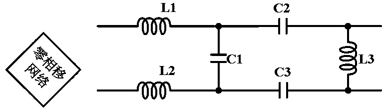
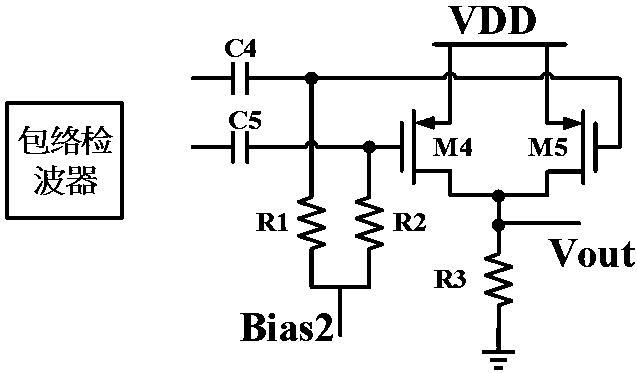
[0018] In module 102, 4 cross-coupled oscillators, 4 zero-phase-shift networks and 4 envelope detectors are included. The internal...


PUM


Abstract

The invention belongs to the technical field of an integrated circuit, and particularly relates to a CMOS integrated circuit terahertz detector applied to a terahertz skin imaging field. A super renewable receiver circuit is adopted by the CMOS integrated circuit terahertz detector; and a circuit structure comprises a low noise amplifier, a group of oscillators and a group of envelope wave detection circuits. A terahertz wave is injected into the low noise amplifier, and is coupled by employing a capacitor alternating current manner; a grid bias voltage is set to be adjustable, and the maximum conversion gain can be obtained by adjusting biases of injection pair transistors; the envelope wave detection outputs a voltage signal positively correlated to the input signal intensity, the injection realizes the sensitivity which is 300GHz to 400GHz and is close to -80dBm, the conversion gain is highest up to 57dB, and the overall power consumption is not greater than 8mW. According to the CMOS integrated circuit terahertz detector related by the invention, the influences of change in a locking range, fluctuation in a center frequency, low output swing and the like due to a technological error and a temperature drift are thoroughly overcome; and the CMOS integrated circuit terahertz detector can be applied to a high-performance terahertz detector.

Description

technical field [0001] The invention belongs to the technical field of integrated circuits, and in particular relates to a CMOS integrated circuit terahertz detector applied in the field of terahertz skin imaging. Background technique [0002] With the development of terahertz technology, terahertz-detection medicine (terahertz-LabMed) is currently receiving great attention. Terahertz wave imaging technology has more unique and more applicable physical characteristics, and the photon energy is low, so it will not be harmful to living things. Molecules, biological cells and tissues produce harmful ionization, the radiation dose is almost zero, and the damage to the human body is very small. It is especially suitable for biopsy of biological tissues and provides a new and reliable technical method for human skin imaging research. [0003] Thanks to the reduction of device size and the further development of technology, CMOS integrated circuits have also entered the millimeter ...

Claims


Application Information

Patent Timeline
Patent Type & Authority Patents(China)
IPC IPC(8): H03B5/12A61B5/00
CPCA61B5/00H03B5/1206
Inventor 任俊彦魏东马顺利陈汧
Owner FUDAN UNIV
Why Eureka
Try Eureka