

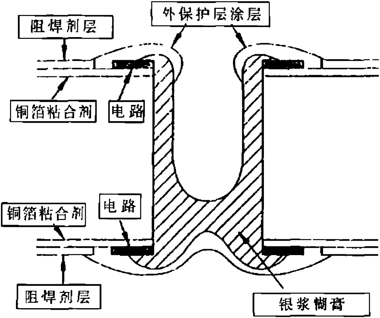
A double-layer through-hole printed circuit board with silver paste through-holes and its manufacturing process
A printed circuit board and through-hole technology, which is applied to printed circuits, printed circuits, printed circuit components, etc., can solve the problems of silver paste migration, insulation resistance drop, etc., to suppress migration, suppress ionization, and improve stability sexual effect
- Summary
- Abstract
- Description
- Claims
- Application Information
AI Technical Summary
Problems solved by technology
Method used
Image

Examples
Embodiment 1
[0027] (1) The surface modification solution is prepared according to the following raw materials in parts by weight: methyltriacetoxysilane 50, zinc acetate 5, stearic monoglyceride 3;
[0028] (2) Immerse the double-layer through-hole printed circuit board with multiple through-holes in the surface modification solution for 2 hours of ultrasonic vibration, and then take it out and dry it in vacuum at 80°C for 5 hours to obtain the double-layer through-hole printed circuit board after surface modification. circuit board;
[0029] (3) Take tolyl cyclohexanone 12, glyceryl tristearate 8, orthosilicate 5, phytic acid ester 4, aminopropyl triethoxysilane 4, methyl isobutyl Ketone 15, mixing the above-mentioned organic matter to obtain a mixed solution, adding silicon dioxide 5, nickel acetate 7 with an average particle diameter of 100nm, magnesium oxide 5 with an average particle diameter of 100nm, and nano-silver powder with an average particle diameter of 50nm in the above-ment...
Embodiment 2
[0034] (1) The surface modification solution is prepared according to the following raw materials in parts by weight: 60 methyltriacetoxysilane, 10 zinc acetate, 8 monoglyceride stearate;
[0035] (2) Immerse the double-layer through-hole printed circuit board with multiple through-holes in the surface modification solution for 5 hours of ultrasonic vibration, and then take it out and dry it in vacuum at 100°C for 2 hours to obtain the surface-modified double-layer through-hole printed circuit board ;
[0036] (3) Take tolyl cyclohexanone 19, glyceryl tristearate 15, tetraethyl orthosilicate 9, phytic acid ester 8, aminopropyl triethoxysilane 6, methyl isobutyl Ketone 22, mixing the above organic matter to obtain a mixed solution, adding 200nm silicon dioxide 13, nickel acetate 12, 500nm magnesium oxide 10, and 100nm silver powder 80 to the above mixed solution according to parts by weight, and stirring evenly to obtain a silver paste;
[0037] (4) Fill the silver paste into ...
Embodiment 3
[0040] (1) The surface modification solution is prepared according to the following raw materials in parts by weight: methyltriacetoxysilane 55, zinc acetate 8, stearic acid monoglyceride 5;
[0041] (2) Immerse the double-layer through-hole printed circuit board with multiple through-holes in the surface modification solution for 3 hours and ultrasonically vibrate for 3 hours, then take it out and dry it in vacuum at 60°C for 6 hours to obtain the surface-modified double-layer through-hole printed circuit board ;
[0042] (3) Take tolyl cyclohexanone 15, glyceryl tristearate 12, tetraethyl orthosilicate 6, phytic acid ester 7, aminopropyl triethoxysilane 5, methyl isobutyl Ketone 19, mixing the above organic matter to obtain a mixed solution, adding 50nm silicon dioxide 11, nickel acetate 10, 60nm magnesium oxide 7, and 20nm silver powder 75 to the above mixed solution according to parts by weight, and stirring evenly to obtain a silver paste;
[0043] (4) Fill the silver pa...
PUM
 Abstract
Description
Claims
Application Information