
Single-face shadow eliminating conductive glass and processing method thereof
A conductive glass and processing method technology, applied in the direction of chemical instruments and methods, glass/slag layered products, electronic equipment, etc., can solve the problems of viewing patterns, affecting electromagnetic shielding, electrostatic protection functions, etc., to achieve simple structure and low cost Low, good electromagnetic shielding effect
- Summary
- Abstract
- Description
- Claims
- Application Information
AI Technical Summary
Problems solved by technology
Method used
Image

Examples
Embodiment Construction
[0022] The present invention will be described below in conjunction with specific embodiments.
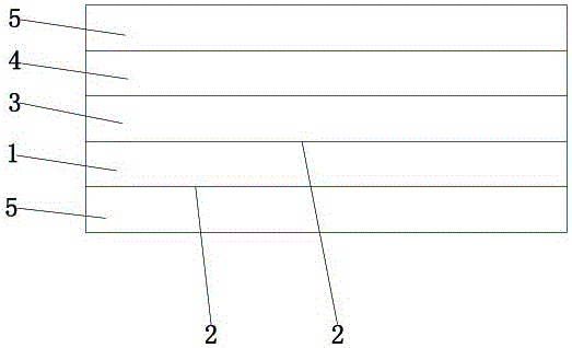
[0023] Such as figure 1 As shown, a single-sided shadow-eliminating conductive glass includes a glass substrate 1, a tin surface 2, an interference layer 3, a transparent passivation layer 4, and an ITO film 5. The upper and lower surfaces of the glass substrate 1 are provided with a tin surface 2, and the glass substrate 1 An interference layer 3 is provided above the tin surface 2 on the upper surface, a transparent passivation layer 4 is provided above the interference layer 3, an ITO mold 5 is provided above the transparent passivation layer 4, and an ITO mold 5 is provided below the tin surface 2 on the lower surface of the glass substrate 1. Film 5.
[0024] As preferred in this embodiment, the interference layer 3 is titanium dioxide.
[0025] As preferred in this embodiment, the transparent passivation layer 4 is silicon dioxide.
[0026] Furthermore, preferably in this ...
PUM
 Abstract
Description
Claims
Application Information