Heterojunction array based ultraviolet detector and manufacturing method thereof

A UV detector and heterojunction technology, applied in semiconductor devices, final product manufacturing, sustainable manufacturing/processing, etc., can solve the problem of photogenerated carrier loss, polycrystalline thin film grain boundary and defect density hindering photogenerated electron diffusion , small area and other issues

Inactive Publication Date: 2016-10-26
兰建龙
View PDF5 Cites 5 Cited by
  • Summary
  • Abstract
  • Description
  • Claims
  • Application Information

AI Technical Summary

Problems solved by technology

[0005] 1. The heterojunction structure of traditional polycrystalline thin film junction devices is similar to that of single crystal junction devices, and the heterojunction interfaces are common planar contacts. Therefore, the area of ​​the space charge region distributed near the contact surface is small, which is harmful to light generation. Limited separation of electron-hole pairs;
[0006] 2. The excessively high grain boundary and defect density in the polycrystalline film seriously hinder the diffusion of photogenerated electrons to the conductive substrate or metal electrode, so that a large number of photogenerated electron-hole pairs are lost due to recombination before they diffuse to the electrode. Lose;
[0007] 3. A large number of defects in the polycrystalline film serve as the recombination center of photogenerated electron-hole pairs, which also seriously reduces the lifetime of photogenerated carriers.
However, the lifetime of photogenerated carriers is limited
Once the diffusion time of photogenerated carriers is longer than its lifetime, this part of photogenerated carriers will be lost

Method used


Image

  • Heterojunction array based ultraviolet detector and manufacturing method thereof
  • Heterojunction array based ultraviolet detector and manufacturing method thereof
  • Heterojunction array based ultraviolet detector and manufacturing method thereof

Examples


Embodiment Construction

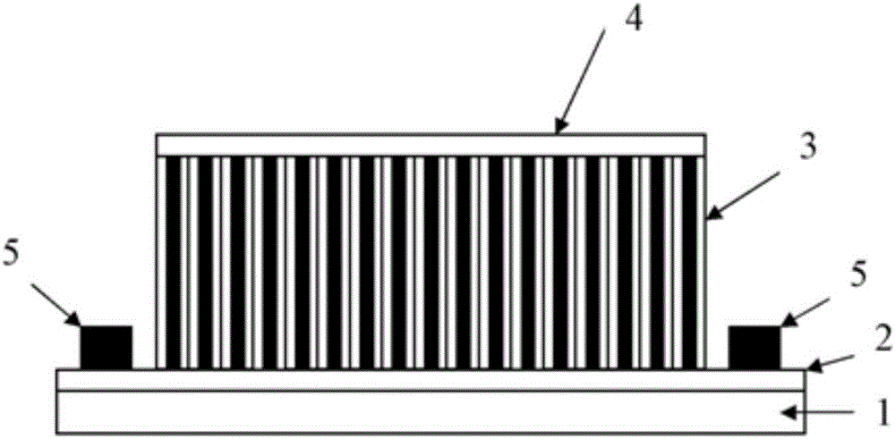
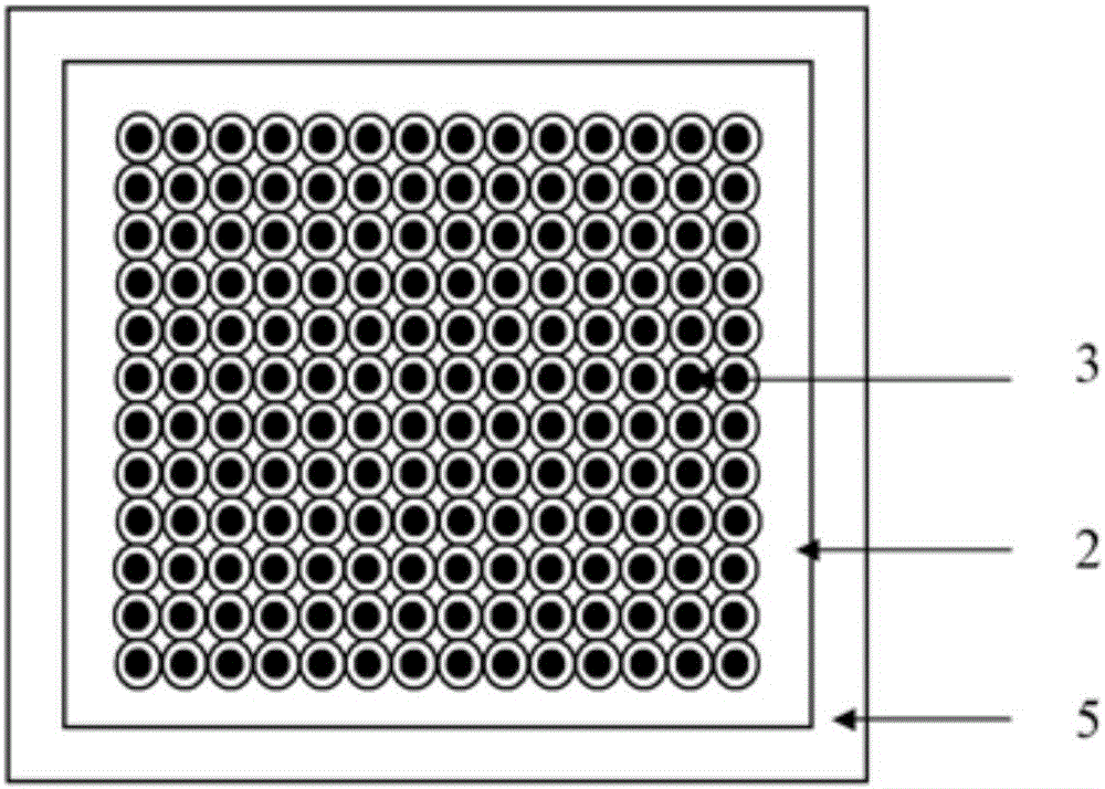
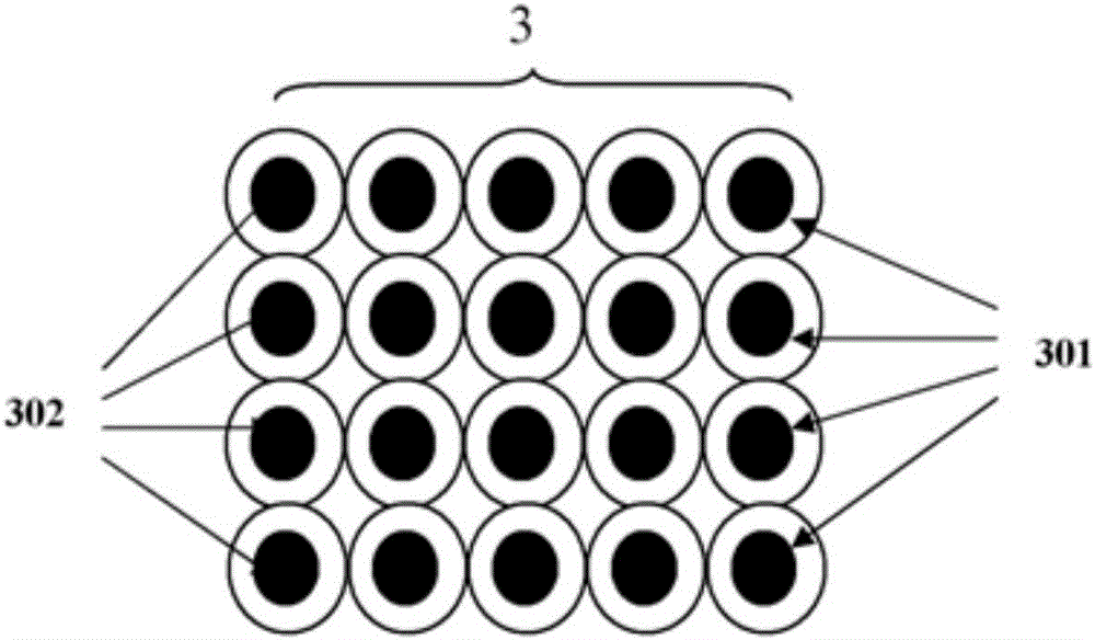
[0041] The present invention will be further described below in conjunction with the accompanying drawings. Such as Figure 1-4 As shown, a heterojunction array-based ultraviolet detector includes a substrate 1 and a conductive film 2, and the conductive film 2 is located on the substrate 1; the substrate 1 is a glass substrate 1, a metal substrate 1 or a silicon substrate 1 , the conductive film 2 has a Sm2O3@ZnO heterojunction array 3 as an ultraviolet light absorbing layer and at least one N-type ohmic electrode 5, and the Sm2O3@ZnO heterojunction array 3 has at least one P-type ohmic electrode Electrode 4; the Sm2O3@ZnO heterojunction array 3 is composed of an array of ZnO nanotubes 301 and Sm2O3 nanowires 302 filled in the ZnO nanotubes 301, and the array of ZnO nanotubes 301 is composed of a growth direction perpendicular to the conductive film 2 ZnO nanotubes 301 are arranged in parallel, and a Sm2O3 nanowire 302 is grown in each ZnO nanotube 301. The conductive film ...


PUM


Abstract

The invention discloses a heterojunction array based ultraviolet detector and a manufacturing method thereof. The detector comprises a substrate and a conductive film; an Sm2O3@ZnO heterojunction array which is used as an ultraviolet absorbing layer and at least one N-type ohmic electrode are arranged on the conductive film; at least one P-type ohmic electrode is arranged on the Sm2O3@ZnO heterojunction array; and the Sm2O3@ZnO heterojunction array is composed of a ZnO nano-tube array and an Sm2O3 nano-wire filled in the ZnO nano-tube. The core structure of the detector provided by the invention is the heterojunction array consisting of the ZnO nano-tube array and the Sm2O3 nano-wire penetrating the ZnO nano-tube; the usage rate of a photo-generated carrier can be sufficiently improved, and the heterojunction array based ultraviolet detector has the advantages of high external quantum efficiency and flexibility, small volume and the like.

Description

technical field [0001] The invention relates to an ultraviolet light detector technology, in particular to a heterojunction array-based ultraviolet light detector for ultraviolet light detection and a preparation method thereof. Background technique [0002] Ultraviolet light detectors have been widely used in military and civilian fields because of their strong anti-interference ability and other advantages. Because traditional single crystal Si-based semiconductor materials have no selective absorption for ultraviolet light, expensive filters must be used, resulting in high production costs for single crystal Si-based ultraviolet detectors, which are difficult to meet the needs of the civilian market. Therefore, at present, people mainly focus on junction devices made of wide bandgap semiconductor materials, such as (Al)GaN, SiC, ZnO, diamond junction devices, etc., and the corresponding research is also mainly concentrated on single crystal devices. Due to the complex pr...

Claims


Application Information

Patent Timeline
Patent Type & Authority Applications(China)
IPC IPC(8): H01L31/109H01L31/0296H01L31/032H01L31/18B82Y30/00B82Y15/00
CPCB82Y15/00B82Y30/00H01L31/0296H01L31/032H01L31/109H01L31/18Y02P70/50
Inventor 兰建龙
Owner 兰建龙
Why Eureka
Try Eureka