Method for preparing molybdenum disulfide thin film by taking GaN as substrate

A molybdenum disulfide and thin-film technology, which is used in the manufacture of semiconductor/solid-state devices, semiconductor devices, electrical components, etc., can solve the problems of uncontrollable electrical properties of devices and inability to meet electronic components, so as to facilitate industrial production and meet quality requirements. , the effect of simple process

Inactive Publication Date: 2016-11-09
SHENZHEN UNIV
View PDF5 Cites 7 Cited by
  • Summary
  • Abstract
  • Description
  • Claims
  • Application Information

AI Technical Summary

Problems solved by technology

When the molybdenum disulfide film prepared by this method is applied to electronic components, the oxide buffer layer in the middle will have an uncontrollable impact on the electrical properties of the device, which cannot meet the requirements of electronic components

Method used


Image

  • Method for preparing molybdenum disulfide thin film by taking GaN as substrate

Examples


Embodiment 1

[0031] 1. Clean the GaN substrate, the cleaning process is as follows:

[0032] 1. Ultrasonic cleaning with acetone and deionized water;

[0033] 2. Ethanol ultrasonic cleaning, deionized water cleaning;

[0034]3. Sulfuric acid: nitric acid = 1:1, cook at 80°C for several minutes, rinse with deionized water;

[0035] 4. Hydrochloric acid: hydrogen peroxide: water = 3:1:1, shake gently for a few minutes, rinse with deionized water;

[0036] 5. Hydrofluoric acid: water = 1:20, shake gently for a few minutes, rinse with deionized water;

[0037] 6. Rinse several times in a beaker of deionized water and rinse with running water.

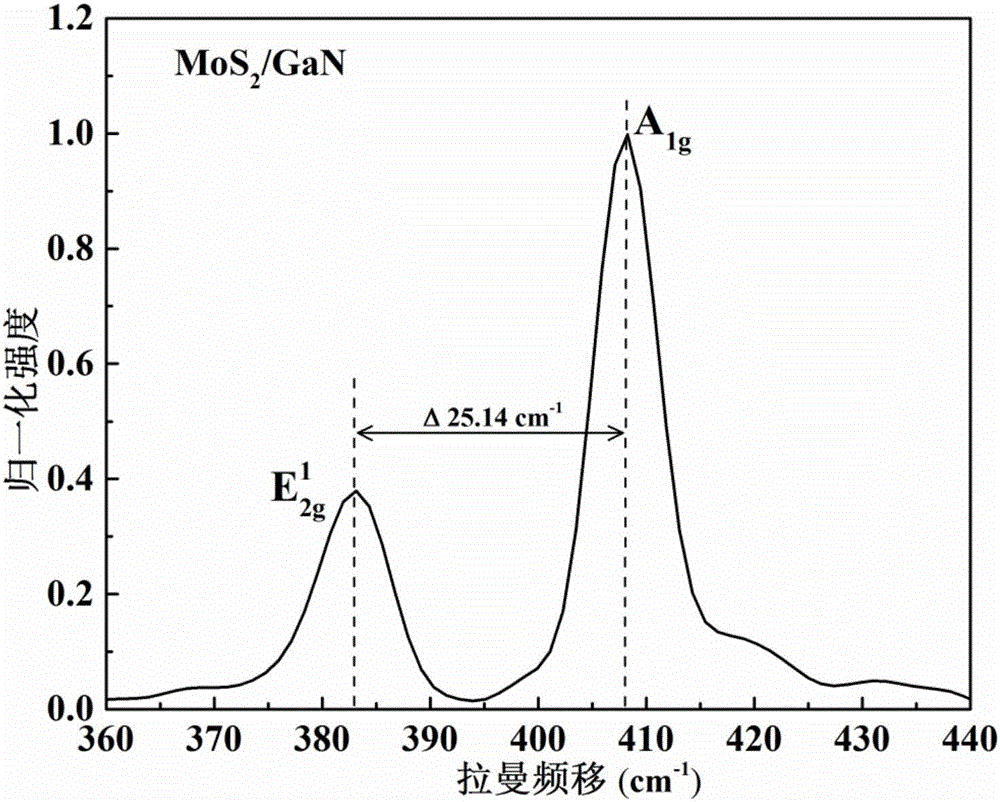
[0038] 2. Using sulfur powder and MoO 3 (99.9%, analytically pure) is the source of sulfur and molybdenum, high-purity argon is used as the carrier gas, and MoS is deposited on GaN by CVD 2 film. The growth temperature is 700° C., the mass of the sulfur source is 0.8 g, the mass of the molybdenum source is 0.04 g, and the pressure is normal pressu...


PUM

PropertyMeasurementUnit
thicknessaaaaaaaaaa
thicknessaaaaaaaaaa
thicknessaaaaaaaaaa

Abstract

The invention is applicable to the technical field of inorganic nano-film materials, and provides a method for preparing a molybdenum disulfide thin film using GaN as a substrate, using GaN as a substrate, and using CVD to generate MoS on the surface of the substrate 2 thin films; the generation of MoS 2 The process of thin film is: with sulfur powder and MoO 3 as the raw material, high-purity argon as the carrier gas, depositing MoS on the substrate 2 film. The present invention also provides a molybdenum disulfide thin film, which is prepared by the above-mentioned preparation method. In the molybdenum disulfide thin film and preparation method thereof provided by the present invention, the bonding force between the molybdenum sulfide material and the substrate material GaN is extremely strong, and the prepared MoS 2 The quality of the thin film is extremely high, which can meet the quality requirements for nano thin film materials in the fields of electricity and optics.

Description

technical field [0001] The invention belongs to the technical field of inorganic nano film materials, in particular to a method for preparing a molybdenum disulfide thin film with GaN as a substrate. Background technique [0002] Molybdenum sulfide thin films are similar to graphene in structure and performance, but unlike graphene, molybdenum sulfide thin films have a tunable band gap. bulk crystalline MoS 2 (Molybdenum disulfide) has a band gap of 1.2eV, and its electronic transition mode is indirect transition; when the thickness is a single layer, MoS 2 The band gap can reach 1.8eV, and its electronic transition mode is changed to direct transition. Therefore, MoS 2 The unique structure, excellent physical properties and adjustable energy bandgap of the thin film make it have more application potential than graphene in the field of electronic devices. It will be a two-dimensional material with very important application prospects in the fields of electricity, optics a...

Claims


Application Information

Patent Timeline
Patent Type & Authority Applications(China)
IPC IPC(8): H01L21/02H01L31/0352
CPCH01L21/02389H01L21/02557H01L21/0262H01L31/0352
Inventor 刘新科李奎龙何佳铸陈乐何祝兵俞文杰吕有明韩舜曹培江柳文军曾玉祥贾芳朱德亮洪家伟
Owner SHENZHEN UNIV
Why Eureka
Try Eureka