Plasma scribing chip packaging structure and manufacturing method

A production method and plasma technology, which is applied in semiconductor/solid-state device manufacturing, electrical components, circuits, etc., can solve problems that affect the dismantling and bonding process, chip drop, and inapplicable temporary bonding packaging solutions, etc., to avoid chip leakage , Easy to hang glue, increase the effect of binding force

Active Publication Date: 2016-11-09
HUATIAN TECH KUNSHAN ELECTRONICS
View PDF12 Cites 12 Cited by
  • Summary
  • Abstract
  • Description
  • Claims
  • Application Information

AI Technical Summary

Problems solved by technology

[0004] At present, people in the field use the PECVD (Physical Vapor Deposition) process, which can better form a dielectric layer on the sidewall of the dicing line and the back of the chip, but the PECVD process uses plasma and high temperature conditions greater than 200 ° C, which is not suitable for temporary The reason for the bonding packaging solution is that plasma or high temperature conditions act on the temporary bonding adhesive to denature the temporary bonding adhesive, which will cause the chip to drop in other processes and affect the subsequent debonding process

Method used


Image

  • Plasma scribing chip packaging structure and manufacturing method
  • Plasma scribing chip packaging structure and manufacturing method
  • Plasma scribing chip packaging structure and manufacturing method

Examples


other Embodiment approach

[0056] In other embodiments, a carrier film is temporarily pasted on the front of the wafer to replace the temporarily bonded carrier. The carrier film has a certain mechanical strength, and one side of the carrier film has a certain adhesive force. Carrier films such as wafer polish films.

[0057] see Figure 4 , under the support of the carrier plate, the back of the wafer is thinned to near the target silicon thickness. Preferably, it is 20 microns to 40 microns thicker than the target silicon. Thinning methods include one or more of grinding, etching, polishing and the like.

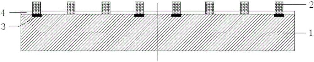
[0058] see Figure 5 , make a mask layer on the back of the thinned wafer, and make an opening at the scribe line position (SL) of the wafer, exposing the silicon substrate at the scribe line position. The mask layer may be a photoresist, and the corresponding opening method is exposure and development.

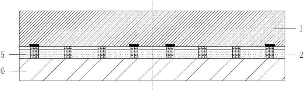
[0059] see Image 6 , plasma dry etching the silicon substrate exposed by the opening, a...

other Embodiment approach

[0064] In other embodiments, a supporting component can be temporarily bonded to the back of the wafer, and the position of the dicing line on the front of the wafer is etched by a plasma dry method to form inclined side walls; the front and side walls of the chip are covered with a passivation layer , removing the passivation layer at the position of the dicing line of the wafer, removing the supporting component on the back, and coating a passivation layer on the back.


PUM

PropertyMeasurementUnit
thicknessaaaaaaaaaa

Abstract

The invention discloses a plasma scribing chip packaging structure and a manufacturing method. The structure comprises a chip, and the front surface of the chip is covered by one dielectric layer. The dielectric layer comprises at least one conductive pad, and at least one side wall of the chip is shaped like a rack which extends in an up / down direction. Moreover, each tooth slot of the rack is shaped like an arc. The side walls and back of the chip are completely coated by a passivation layer. In the structure, the passivation layer wraps the back and side walls of the chip, thereby avoiding the electric leakage, caused by the exposing of the base body of the chip, of the chip. The side walls of the chip are shaped like the rack, thereby facilitating the hanging and gluing, and increasing the binding force of the passivation layer with the side walls. The method employs a plasma dry method for etching, scribing and segmenting of a wafer, solves a problem of edge breakage when a blade mechanically cuts the chip, also solves a problem that the side walls of the chip are exposed because of a plasma separation method, and improves the feasibility of the technology.

Description

technical field [0001] The invention relates to the technical field of semiconductor packaging, in particular to a plasma dicing chip packaging structure and a manufacturing method. Background technique [0002] In the wafer-level packaging process of semiconductor chips, after the packaging is completed, they are cut and separated into individual chips, which has high packaging efficiency and low cost. Cutting is usually done mechanically with a blade, which is prone to edge chipping and takes a long time to cut, which affects production capacity. [0003] Plasma removes the barrier material at the dicing line of the wafer, mainly silicon, and the method of separating and forming a single chip is an ideal separation method from the perspective of chipping and production capacity. However, the silicon on the sidewall of the chip after plasma separation will be exposed, which will easily lead to leakage and lead to chip failure. Therefore, how to protect packaged chips in a...

Claims


Application Information

Patent Timeline
Patent Type & Authority Applications(China)
IPC IPC(8): H01L21/78H01L21/56H01L21/3065
CPCH01L21/3065H01L21/561H01L21/78H01L21/7806
Inventor 于大全范俊
Owner HUATIAN TECH KUNSHAN ELECTRONICS
Why Eureka
Try Eureka