

A method for preparing thick layer epitaxy on thin SB substrate for vdmos device
A substrate and device technology, applied in the field of silicon epitaxial layer preparation process for VDMOS devices, can solve the problems of increased difficulty in controlling epitaxial thickness uniformity, increased epitaxial debris rate, chipping, slip lines, etc., and achieve edge crystallization quality Good, improve processing yield, good effect of thickness uniformity
- Summary
- Abstract
- Description
- Claims
- Application Information
AI Technical Summary
Problems solved by technology
Method used
Image

Examples
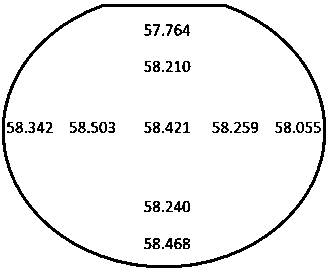
Embodiment 1
[0022] Step 1: The bottom end of the induction coil under the graphite base of the epitaxial furnace has 9 groups of adjustable distance adjustment rods, named 4#~12# respectively. The position of the coil is raised or lowered by rotating the adjustment rod to adjust the coil The distance between each part and the graphite base of the epitaxial furnace improves the temperature uniformity of the graphite base of the epitaxial furnace. The scale value of the 4# adjustment rod is set to -10, and the scale value of the 5# adjustment rod is set to- The scale value of 15, 6# adjustment rod is set to -30, the scale value of 7# adjustment rod is set to -30, the scale value of 8# adjustment rod is set to 0, and the scale value of 9# adjustment rod is set to The scale value of -30, 10# adjustment rod is set to -30, the scale value of 11# adjustment rod is set to +3, and the scale value of 12# adjustment rod is set to +3.
[0023] Step 2: Use hydrogen chloride (HCl) to etch and polish the g...
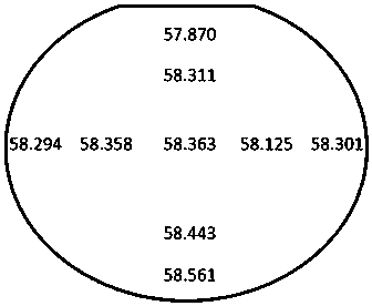
Embodiment 2
[0032] Step 1: The bottom end of the induction coil under the graphite base of the epitaxial furnace has 9 groups of adjustable distance adjustment rods, named 4#~12# respectively. The position of the coil is raised or lowered by rotating the adjustment rod to adjust the coil The distance between each part and the graphite base of the epitaxial furnace to improve the temperature uniformity of the graphite base of the epitaxial furnace. The scale value of the 4# adjustment rod is set to -8, and the scale value of the 5# adjustment rod is set to- The scale value of 13,6# adjustment rod is set to -28, the scale value of 7# adjustment rod is set to -28, the scale value of 8# adjustment rod is set to +2, and the scale value of 9# adjustment rod is set For -29, the scale value of 10# adjusting rod is set to -30, the scale value of 11# adjusting rod is set to +2, and the scale value of 12# adjusting rod is set to +2.
[0033] Step 2: Use hydrogen chloride gas (HCl) to polish the graphit...
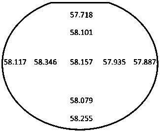
Embodiment 3
[0042] Step 1: The bottom end of the induction coil under the graphite base of the epitaxial furnace has 9 groups of adjustable distance adjustment rods, named 4#~12# respectively. The position of the coil is raised or lowered by rotating the adjustment rod to adjust the coil The distance between each part and the graphite base of the epitaxial furnace, thereby improving the temperature uniformity of the graphite base of the epitaxial furnace, the scale value of 4# adjusting rod is set to -7, and the scale value of 5# adjusting rod is set to- The scale value of 13,6# adjustment rod is set to -28, the scale value of 7# adjustment rod is set to -30, the scale value of 8# adjustment rod is set to +2, and the scale value of 9# adjustment rod is set to The scale value of -27, 10# adjustment rod is set to -27, the scale value of 11# adjustment rod is set to +1, and the scale value of 12# adjustment rod is set to +1;
[0043] Step 2: Use hydrogen chloride (HCl) to polish the graphite ba...
PUM
| Property | Measurement | Unit |
|---|---|---|
| thickness | aaaaa | aaaaa |
| thickness | aaaaa | aaaaa |
Abstract
Description
Claims
Application Information