Organic electroluminescent material and organic electroluminescent device
An electroluminescent and organic technology, applied in the field of luminescent materials and light-emitting devices, can solve the problems of low luminous efficiency and high triplet energy gap of light-emitting devices, and achieve the effect of increasing luminous efficiency and thermal stability
- Summary
- Abstract
- Description
- Claims
- Application Information
AI Technical Summary
Problems solved by technology
Method used
Image

Examples
no. 1 example
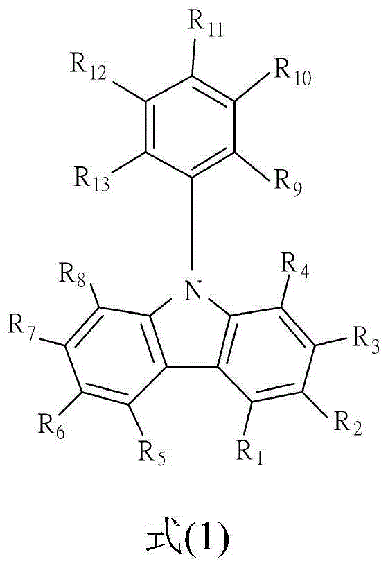
[0038] The organic electroluminescent material according to the first embodiment of the present invention has the following structure of formula (1).
[0039]
[0040] The structure of the above formula (1) is a polycyclic nitrogen-containing heterocyclic organic compound, when R 2 , R 4 , R 6 , R 9 or R 13 When all are independently independent hydrogen atoms, the structure of formula (1) is N-phenylcarbazole (N-phenylcarbazole, NPC), which belongs to carbazole derivatives, or called carbazole group. And in this example, R 2 , R 4 , R 6 , R 9 or R 13 One or both of them can be independent triazole derivatives respectively, and the triazole derivatives described in this embodiment are derivatives having the structure of the following formula (2).
[0041]
[0042] That is to say, this embodiment utilizes the nitrogen atom on the triazole derivative to be connected to R on the N-phenylcarbazole 2 , R 4 , R 6 , R 9 or R 13 One or two of them to form a double ...
no. 2 example
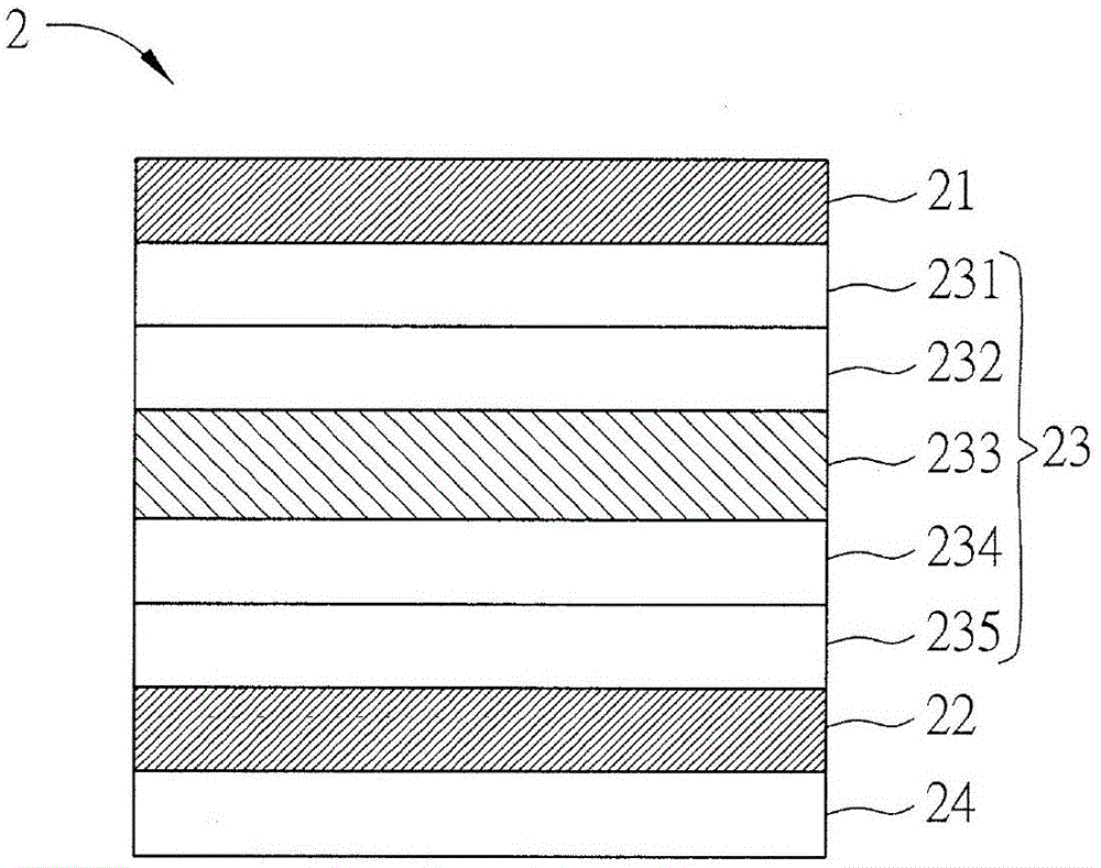
[0051] figure 2 is a schematic diagram of the organic electroluminescent device of the second embodiment of the present invention, please refer to figure 2 shown. The organic electroluminescent device 2 of this embodiment includes a first electrode layer 21, a second electrode layer 22, and an organic light emitting unit 23, wherein the organic light emitting unit 23 is disposed on the first electrode layer 21 and the second electrode layer 22 between. Wherein, the organic light-emitting unit 23 includes at least one organic electroluminescent material, and the organic electroluminescent material is the organic electroluminescent material (carbazole derivative) described in the first embodiment, so its details can refer to the first embodiment For example, no further details are given here.
[0052]In this embodiment, the first electrode layer 21 is disposed on a substrate 24, wherein the substrate 24 is selected from at least one of a rigid substrate, a flexible substrat...
Embodiment 1
[0064] Embodiment one : Synthesis of Compound O-1
[0065]
[0066] Take carbazole (compound 1, 0.30g, 1.8mmol), 1-fluoro-3-nitrobenzene (1-fluoro-3-nitrobenzene, 0.25g, 1.8mmol), dimethylsulfoxide (dimethylsulfoxide, 5mL) Put into a single-necked bottle (10mL). After stirring with a magnetic stirring bar until the solid was dissolved, cesium carbonate (0.64 g, 2.0 mmol) was added and reacted at room temperature for 18 hours. Then, after adding deionized water (5mL), a yellow solid was produced, which was extracted three times with chloroform (30mL), the organic layer was collected and washed three times with deionized water (30mL), and the organic layer was dried with anhydrous magnesium sulfate , and then concentrated by gyratory to remove the solvent and compound 2 (0.49 g) was obtained with a yield of 94%.
[0067] Next, take compound 2 (2.0g, 6.9mmol), tin(II) chloride dihydrate (tin(II) chloride dihydrate, 7.83g, 34.7mmol), ethyl acetate (34.5mL), ethanol (ethanol...
PUM
| Property | Measurement | Unit |
|---|---|---|
| Thickness | aaaaa | aaaaa |
| Thickness | aaaaa | aaaaa |
| Thickness | aaaaa | aaaaa |
Abstract
Description
Claims
Application Information
 - Generate Ideas
- Intellectual Property
- Life Sciences
- Materials
- Tech Scout
- Unparalleled Data Quality
- Higher Quality Content
- 60% Fewer Hallucinations
Browse by: Latest US Patents, China's latest patents, Technical Efficacy Thesaurus, Application Domain, Technology Topic, Popular Technical Reports.
© 2025 PatSnap. All rights reserved.Legal|Privacy policy|Modern Slavery Act Transparency Statement|Sitemap|About US| Contact US: help@patsnap.com