
Method and system for achieving enhanced HEMT device through electrochemical corrosion

An enhanced, electrochemical technology, applied in electrical components, semiconductor devices, semiconductor/solid-state device manufacturing, etc., can solve problems such as affecting device stability, difficult recessed gate structure process, and degrading device performance, to improve repeatability, Easy to mass-produce, less etching damage

Active Publication Date: 2016-11-23
SUZHOU NENGWU ELECTRONICS TECH
View PDF5 Cites 2 Cited by
  • Summary
  • Abstract
  • Description
  • Claims
  • Application Information

AI Technical Summary

Problems solved by technology

At present, the main methods for realizing enhanced HEMT devices include thin barrier layer, concave gate structure, P-type capping layer and F treatment, etc., but each technology has its own shortcomings.
For example, the world's first enhancement mode HEMT device is realized by using a thinner barrier layer. This method does not use an etching process, so the damage caused is small, but due to the thinner barrier layer, the saturation of the device The current is small; the P-type capping layer does not require an etching process, but a more serious interface state is generated, which affects the stability of the device; F plasma treatment can also realize an enhanced HEMT device, and does not require etching, but the F plasma The barrier layer is also etched during the implantation process, resulting in a decrease in device performance
[0004] In these methods of realizing enhanced HEMT devices, because GaN materials have good etching resistance characteristics, common acids such as sulfuric acid, hydrochloric acid, nitric acid, etc. and common alkalis such as potassium hydroxide, sodium hydroxide, etc. cannot Efficient etching of GaN, and so far, no one has been able to achieve Al x Ga (1-x) A solution with high selective etching ratio for N(0<x≤1) and GaN materials
Therefore, in the formation process of the traditional concave gate structure, the barrier layer under the gate is mainly realized by plasma (mainly chlorine-based plasma) etching method, and the barrier layer of a general HEMT device is only 20-30nm , so the etching of the concave gate faces problems such as the control of the etching thickness and the repair of the etching damage. The process of forming the concave grid structure by the etching process is difficult to control and the repeatability is poor.

Method used


Image

  • Method and system for achieving enhanced HEMT device through electrochemical corrosion
  • Method and system for achieving enhanced HEMT device through electrochemical corrosion
  • Method and system for achieving enhanced HEMT device through electrochemical corrosion

Examples


Embodiment Construction

[0037] The technical solutions of the embodiments of the present invention will be clearly and completely described below in conjunction with the accompanying drawings of the present invention.

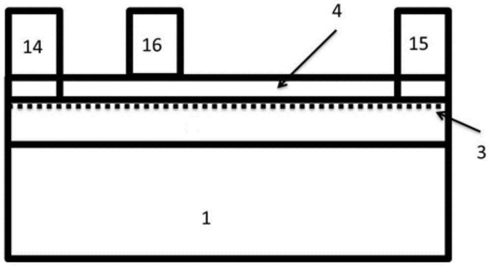
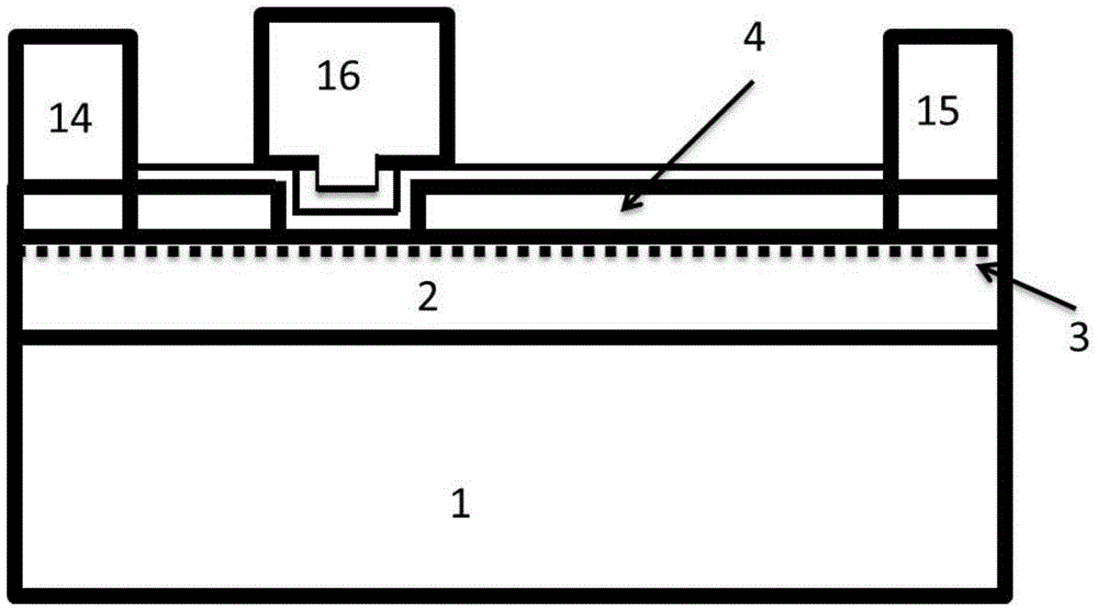
[0038] Such as figure 1 As shown, for common HEMT devices (taking AlGaN / GaN devices as an example), generally speaking, when zero bias voltage or no bias voltage is applied to the gate electrode 16, both the source electrode 14 and the drain electrode 15 are connected to the two-dimensional electron gas 3-phase connection, so the source electrode 14 and the drain electrode 15 of the HEMT device are turned on, and the HEMT device is in the open state. Generally, this kind of HEMT device is called a depletion HEMT device, and it can also be called a normally-on HEMT device. In order to make the HEMT device in the off state, the two-dimensional electron gas 3 between the source electrode 14 and the drain electrode 15 must be depleted or the two-dimensional electron gas in a certain regio...


PUM


Abstract

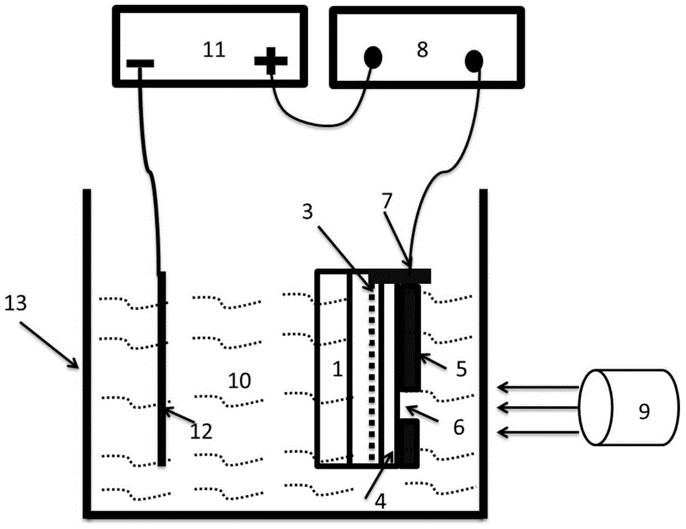
The invention discloses a system for achieving an enhanced HEMT device through electrochemical corrosion. The system comprises an etching light source, an etching power supply, an etching solution, a cathode plate and an etching sample, wherein the etching solution, the cathode plate, the etching power supply and the etching sample are connected in series to form an etching loop; a barrier layer Al*Ga(1-x)N, located at the lower end of a gate electrode of the device, of the etching sampling is completely etched through an electrochemical method; and the polarization effect of the barrier layer is weakened to exhaust a two-dimensional electron gas, so that the condition that the HEMT device is in an off state at zero gate bias voltage is achieved and transformation of a normally open HEMT device into a normally closed HEMT device is achieved. The invention further discloses an electrochemical etching method for achieving the enhanced HEMT device. An enhanced HEMT is effectively achieved, the system has the characteristics of being simple in process, high in repeatability, low in cost, small in etching damage and the like, and massive production is easy to implement.

Description

technical field [0001] The invention relates to an enhanced HEMT device, in particular to a method and system for realizing an enhanced HEMT device through electrochemical corrosion. Background technique [0002] HEMT devices are made by making full use of the two-dimensional electron gas formed by the heterojunction structure of semiconductors. Compared with III-VI (such as AlGaAs / GaAs HEMT devices), III-nitride semiconductors are due to piezoelectric polarization and spontaneous The polarization effect, on the heterostructure (Heterostructure), such as: AlGaN / GaN, can form a high concentration of two-dimensional electron gas. Therefore, in HEMT devices made of group III nitrides, the barrier layer generally does not need to be doped. Group III nitrides have the characteristics of large band gap, high saturated electron drift velocity, high critical breakdown electric field and strong radiation resistance, which can meet the requirements of higher power and higher power de...

Claims


Application Information

Patent Timeline
IPC IPC(8): H01L21/335H01L21/28
Inventor 蔡勇张志利张宝顺付凯于国浩孙世闯宋亮
Owner SUZHOU NENGWU ELECTRONICS TECH
Learn More