Supercharge Your Innovation With Domain-Expert AI Agents!

Fin-type field-effect transistor with Omega-shaped top gate structure and preparation method of fin-type field-effect transistor

A fin field effect and transistor technology, which is applied in semiconductor/solid-state device manufacturing, semiconductor devices, electrical components, etc., can solve the problems of lack of top gate channel cross-sectional area, small equivalent Fin thickness, large leakage current, etc. The effect of low cost, high on-state current, and small source-drain series resistance

Inactive Publication Date: 2016-11-23
PEKING UNIV
View PDF4 Cites 2 Cited by
  • Summary
  • Abstract
  • Description
  • Claims
  • Application Information

AI Technical Summary

Problems solved by technology

For the triangular Fin, because the top Fin is thinner, it has a smaller equivalent Fin thickness and stronger gate control capability, so it has a smaller leakage current, but it lacks a top gate and the channel cross-sectional area is small, and the drive current On the other hand, the rectangular Fin is opposite, the equivalent Fin thickness is relatively large, the gate control ability is weaker than the triangular Fin, and the leakage current is large, but because the rectangular Fin has a top gate, and the top gate can contribute a considerable part of the drive current to the device, and The channel cross-sectional area of ​​the rectangular Fin is also larger, so the driving current will be much higher than that of the triangular Fin

Method used


Image

  • Fin-type field-effect transistor with Omega-shaped top gate structure and preparation method of fin-type field-effect transistor
  • Fin-type field-effect transistor with Omega-shaped top gate structure and preparation method of fin-type field-effect transistor
  • Fin-type field-effect transistor with Omega-shaped top gate structure and preparation method of fin-type field-effect transistor

Examples


Embodiment Construction

[0082] The present invention will be described in detail below in conjunction with the accompanying drawings and specific examples.

[0083] The preparation of N-type Ω-type top-gate structure fin field-effect transistors on SOI substrates can be realized according to the following steps:

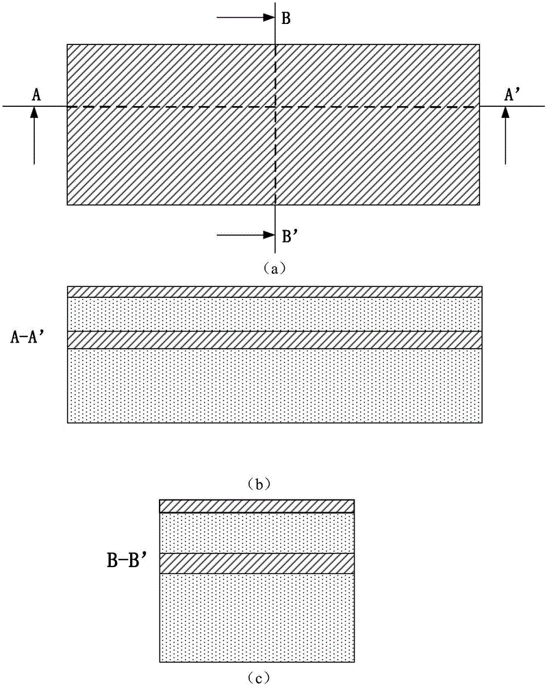
[0084] 1) On the P-type (100) SOI substrate, the top silicon film will be thinned to 250nm by HNA solution, LPCVDSiO 2 100nm as mask layer 1, such as figure 1 shown;

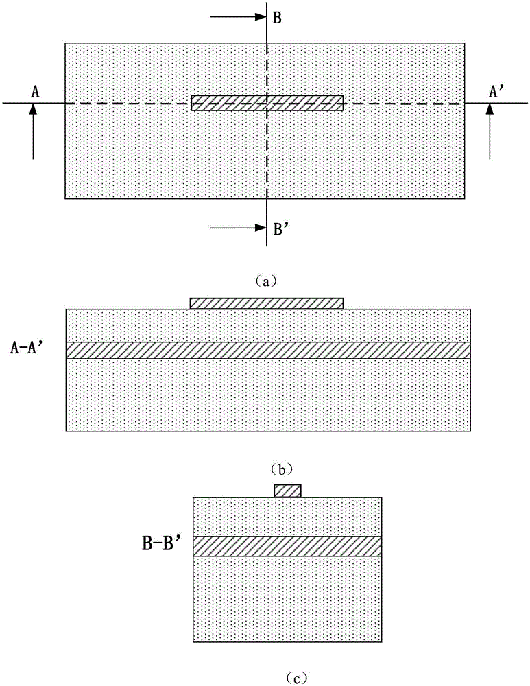
[0085] 2) Define the mask pattern of the channel region with a length of 100nm and a width of 50nm by electron beam lithography, that is, the line width of the top of the Ω-type Fin is 50nm, using photoresist as a mask, and ICP etching mask layer 1 to form a rectangular Fin mask film, the line width of the rectangular Fin mask is 50nm, which is the line width at the top of the Ω-type Fin, and the adhesive is removed, such as figure 2 shown;

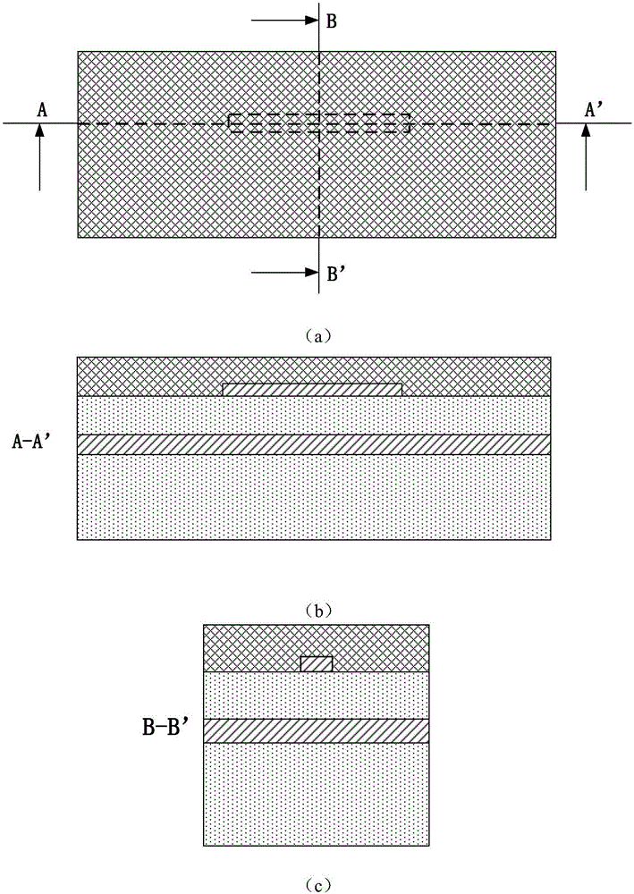
[0086] 3) LPCVD 300nm silicon nitride is used as the mask layer 2, the mask la...


PUM


Abstract

The invention provides a fin-type field-effect transistor with an Omega-shaped top gate structure and a preparation method of the fin-type field-effect transistor, and belongs to the technical field of manufacturing of super-large-scale integrated circuits. According to the invention, a rectangular top gate is changed into an Omega-shaped top gate; the gate control ability of the Omega-shaped gate structure is close to that of a fence structure, so that the gate control ability of the Omega-shaped top gate FinFET to a 1 / 3 position on Fin must be higher than that of a rectangular top gate FinFET, thus leakage current of the Omega-shaped top gate FinFET is smaller than that of a traditional FinFET; the cross-sectional area of a channel in the 1 / 3 position on Fin of the Omega-shaped top gate FinFET is not reduced. Compared with the traditional fin-type field-effect transistor, the fin-type field-effect transistor provided by the invention can obtain higher on-state current, and is compatible with the traditional integrated circuit manufacturing technology, simple in process and low in cost.

Description

technical field [0001] The invention belongs to the technical field of ultra-large-scale integrated circuit manufacturing, and relates to an Ω-shaped top gate structure fin field effect transistor and a preparation method thereof. Background technique [0002] When semiconductor devices enter the 22nm technology generation, Fin Field Effect Transistor (FinFET) has become the mainstream of semiconductor devices due to its outstanding ability to suppress short-channel effects, high integration density, and compatibility with traditional CMOS processes. The Fin structure of an ideal FinFET should be a standard rectangle or square. However, due to the reliability hazards at sharp corners and the limitations of process conditions, the actual Fin of a FinFET will not be an ideal shape. For example, Intel adopts a triangular-like Fin with a small top and a large bottom at the 22nm technology node, and when releasing the next-generation FinFET of the 14nm technology node, the Fin st...

Claims


Application Information

Patent Timeline
Patent Type & Authority Applications(China)
IPC IPC(8): H01L29/78H01L21/336
CPCH01L29/7853H01L29/66795H01L29/7854
Inventor 黎明陈珙张嘉阳黄如
Owner PEKING UNIV
Features
  • R&D
  • Intellectual Property
  • Life Sciences
  • Materials
  • Tech Scout
  • Unparalleled Data Quality
  • Higher Quality Content
  • 60% Fewer Hallucinations
Learn More