Formation method of semiconductor structure

A semiconductor and plasma technology, which is applied in semiconductor/solid-state device manufacturing, electrical components, circuits, etc., can solve the problems that the electrical properties of semiconductor structures need to be improved, and achieve improved reliability and electrical properties, improved quality, and consistent opening depths Effect

Active Publication Date: 2020-03-10
SEMICON MFG SOUTH CHINA CORP +1
View PDF4 Cites 0 Cited by
  • Summary
  • Abstract
  • Description
  • Claims
  • Application Information

AI Technical Summary

Problems solved by technology

[0004] However, the electrical properties of semiconductor structures formed by existing technologies still need to be improved

Method used


Image

  • Formation method of semiconductor structure
  • Formation method of semiconductor structure
  • Formation method of semiconductor structure

Examples


Embodiment Construction

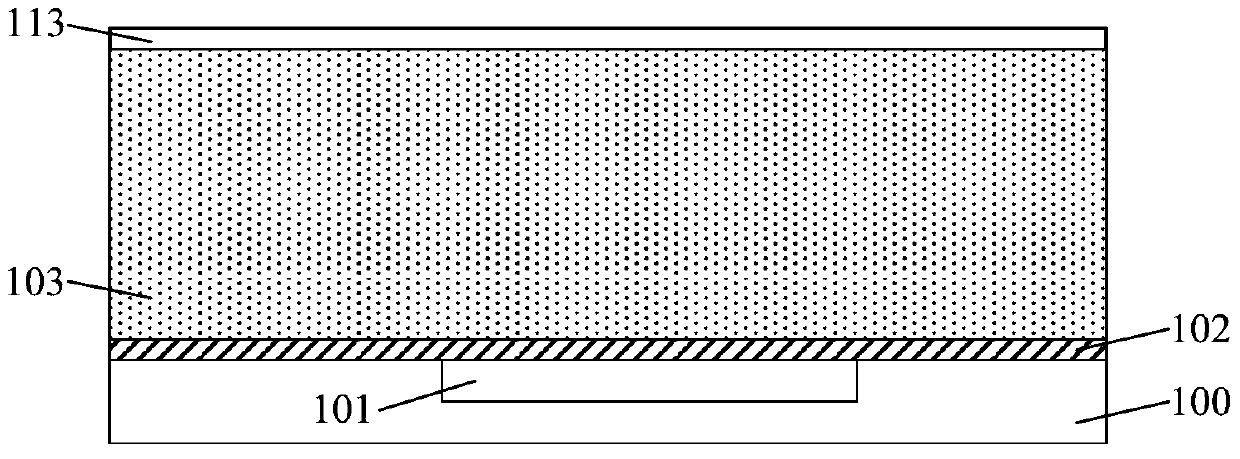
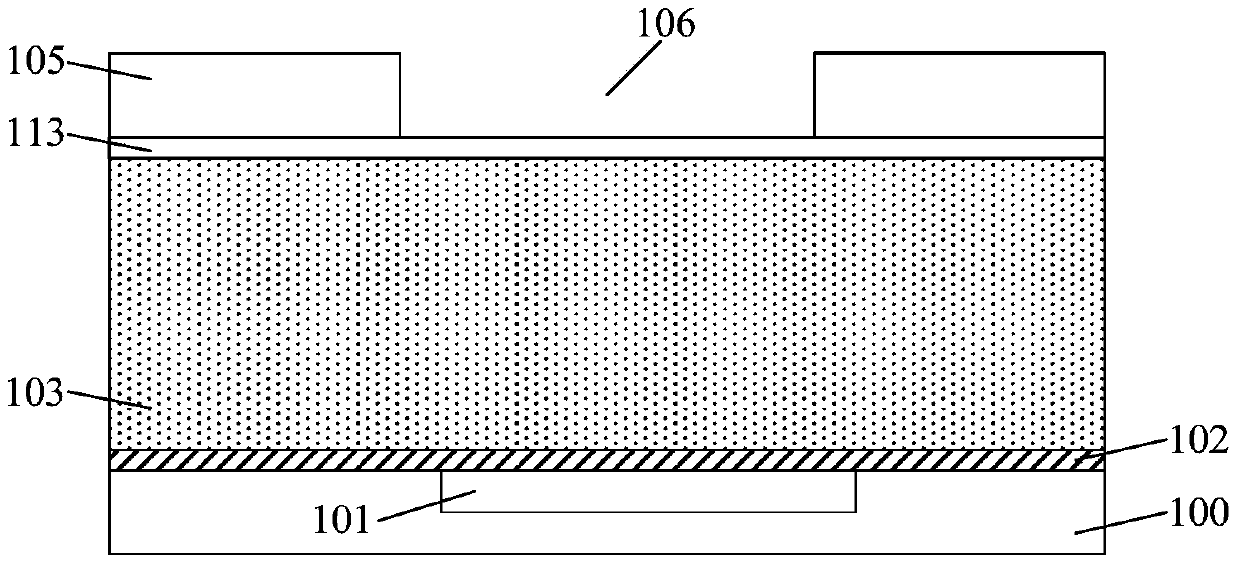
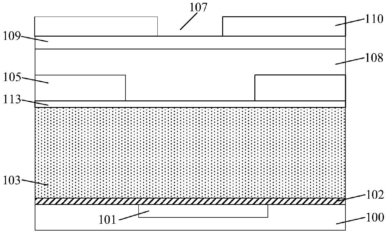
[0030] It can be seen from the background art that the electrical performance of the semiconductor structure formed in the prior art needs to be improved. For example, the breakdown voltage (VBD: Breakdown Voltage) of the semiconductor structure is low, and there is a time-dependent dielectric breakdown (TDDB: TimeDependent Dielectric Breakdown) problem.

[0031] It has been found through research that the dielectric layer is usually etched by a dry etching process to form an opening through the dielectric layer. During the dry etching process, impurities will be introduced into the opening, such as the reaction between the etching gas and the dielectric layer to generate reaction by-products. The product, the etching gas and the mask layer material (such as photoresist, organic distribution material, anti-reflection material) react to form reaction by-products, and part of the reaction by-products will fall on the bottom of the opening and the sidewall of the opening.

[0032]...


PUM

PropertyMeasurementUnit
thicknessaaaaaaaaaa
thicknessaaaaaaaaaa
relative permittivityaaaaaaaaaa

Abstract

Disclosed is a formation method for a semiconductor structure. The formation method comprises the steps of providing a substrate and a dielectric layer which is positioned on the surface of the substrate, wherein a bottom layer metal layer is formed in the substrate; etching the dielectric layer to form an opening which runs through the dielectric layer, wherein the surface of the bottom layer metal layer is exposed out of the bottom of the opening; performing etching post-processing on the opening by adopting an H<2>-containing gas; forming a silicon layer on the surface of the side wall of the opening after the etching post-processing is carried out; after the silicon layer is formed, performing wet cleaning processing on the opening; and forming a conductive layer, wherein the opening is filled with the conductive layer. By adoption of the formation method, when the impurities in the opening are removed, corrosion to the dielectric layer on the side wall of the opening is avoided in the process of the wet cleaning processing, so that the breakdown voltage is increased; the time dependent dielectric breakdown problem is restrained; and the reliability and the electrical performance of the semiconductor structure are improved.

Description

technical field [0001] The invention relates to the technical field of semiconductor manufacturing, in particular to a method for forming a semiconductor structure. Background technique [0002] With the continuous advancement of VLSI process technology, the feature size of semiconductor devices has been continuously reduced, and the chip area has continued to increase. The delay time of the interconnect structure can be compared with the device gate delay time. People are faced with the problem of how to overcome the significant increase in RC (R refers to resistance, C refers to capacitance) delay due to the rapid increase in connection length. In particular, due to the increasing influence of the capacitance between metal wirings, the performance of the device is greatly reduced, which has become a key restrictive factor for the further development of the semiconductor industry. In order to reduce the RC delay caused by interconnection, various measures have been adopted...

Claims


Application Information

Patent Timeline
Patent Type & Authority Patents(China)
IPC IPC(8): H01L21/768
Inventor 张海洋周俊卿
Owner SEMICON MFG SOUTH CHINA CORP
Why Eureka
Try Eureka