Metal oxide semiconductor diode with multiple accumulation layers

An oxide semiconductor and accumulation layer technology, applied in semiconductor devices, electrical components, circuits, etc., can solve the problems of high forward conduction voltage drop and low conduction voltage drop, and achieve lower forward conduction voltage drop and low conduction voltage. The effect of reducing the on-voltage and forward voltage drop

Inactive Publication Date: 2016-12-14
UNIV OF ELECTRONICS SCI & TECH OF CHINA
View PDF5 Cites 3 Cited by
  • Summary
  • Abstract
  • Description
  • Claims
  • Application Information

AI Technical Summary

Problems solved by technology

[0004] The purpose of the present invention is to solve the problem of high forward conduction voltage drop of shallow groove metal oxide diodes in the medium and high voltage field, so that the device can achieve low conduction voltage drop while ensuring a high reverse withstand voltage

Method used


Image

  • Metal oxide semiconductor diode with multiple accumulation layers
  • Metal oxide semiconductor diode with multiple accumulation layers
  • Metal oxide semiconductor diode with multiple accumulation layers

Examples


Embodiment 1

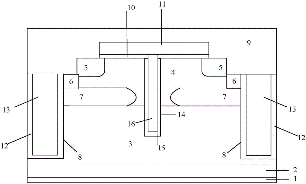
[0018] Such as figure 1 As shown, a multi-accumulation layer metal oxide semiconductor diode in this example includes an anode electrode 9, an N-doped region 4, an N-type region 3, and an N-type heavily doped single crystal stacked sequentially from top to bottom. Silicon substrate 2 and cathode electrode 1; the two ends of the anode electrode 9 extend vertically downwards into the N-doped region 4, and the N-doped region 4 has an N-type heavily doped region 5, and the N-type The upper surface of the heavily doped region 5 is in contact with the anode electrode 9, and the side of the N-type heavily doped region 5 is in contact with the part where the anode electrode 9 extends into the N-doped region 4; the N-type heavily doped regions 5 on both sides The upper surface of the N-doped region 4 in between has a planar gate structure, the planar gate structure is located in the anode electrode 9, and the planar gate structure includes a gate oxide layer 10 and a doped polysilicon ...

Embodiment 2

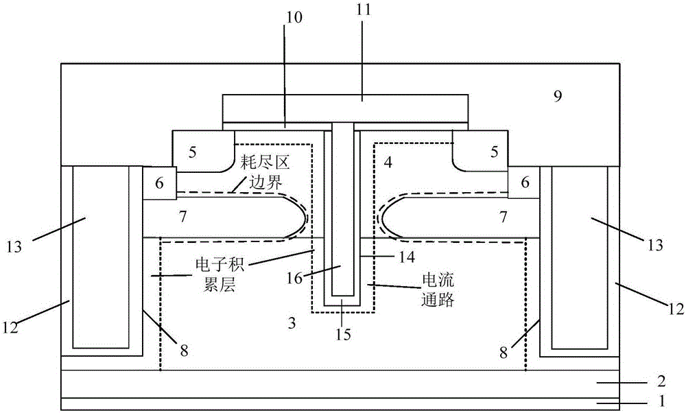
[0028] Such as Figure 6 As shown, the structure of this example is based on Embodiment 1, the depth of the first groove 8 and the second groove 14 is increased, so that the first dielectric layer 12 and the second dielectric layer 15 are connected to the substrate 2 . The beneficial effect of this example is that the length of the electron accumulation layer is extended, and the forward conduction voltage drop of the device can be further reduced.


PUM


Abstract

The invention relates to the technical field of semiconductor devices, specifically to a metal oxide semiconductor diode with multiple accumulation layers. Multiple electron accumulation layers are formed in a drift region during forward conduction of a device, so that a forward conduction voltage drop of the device is effectively reduced. Reverse blocking voltage of the device is improved by introducing a transverse electric field into the drift region of the device during reverse blocking, so that the diode with high withstand voltage and a low conduction voltage drop is achieved.

Description

technical field [0001] The invention belongs to semiconductor technology, in particular to a metal oxide semiconductor diode with multiple accumulation layers. Background technique [0002] Diodes are one of the most commonly used electronic components. Traditional rectifier diodes are mainly Schottky rectifiers and PN junction rectifiers. Among them, the PN junction diode can withstand a high reverse blocking voltage and has good stability, but its forward conduction voltage drop is relatively large, and its reverse recovery time is relatively long. Schottky diodes are manufactured using the principle of metal-semiconductor junctions formed by metal-semiconductor contacts, and the on-state voltage drop is low. Due to the conduction of unipolar carriers, Schottky diodes have no excess minority carrier accumulation during forward conduction, and the reverse recovery is relatively fast. However, the reverse breakdown voltage of the Schottky diode is low, the reverse leakage ...

Claims


Application Information

Patent Timeline
Patent Type & Authority Applications(China)
IPC IPC(8): H01L29/41H01L29/423H01L29/861
CPCH01L29/42316H01L29/41H01L29/861
Inventor 任敏林育赐谢驰苏志恒李泽宏张金平高巍张波
Owner UNIV OF ELECTRONICS SCI & TECH OF CHINA
Why Eureka
Try Eureka