

A kind of hemt epitaxy structure and preparation method
A technology of epitaxial structure and barrier layer, which is applied in the field of HEMT epitaxy, can solve the problems such as the difficulty of independent control of the conductivity of multiple channels, the difficulty of multi-channel HEMT, and the limitation of output power, so as to avoid memory effects and improve leakage , The effect of increasing the knee point voltage
Inactive Publication Date: 2019-08-02
INST OF SEMICONDUCTORS - CHINESE ACAD OF SCI
View PDF2 Cites 0 Cited by
- Summary
- Abstract
- Description
- Claims
- Application Information
AI Technical Summary
Problems solved by technology
[0003] In addition, common HEMT epitaxy is single-channel conduction, which limits the improvement of output power
Existing multi-channel HEMTs often introduce InGaN barrier layers or carry out n-type doping, etc., but the growth temperature of InGaN is much lower than that of AlGaN, and doping also increases the process complexity. Therefore, it is difficult to prepare multi-channel HEMTs by these methods Larger and difficult to independently control the conductivity of multiple channels
Method used
View moreImage
Smart ImageViewing Examples

Examples
preparation example Construction
[0029] About the preparation method of the HEMT epitaxial structure:
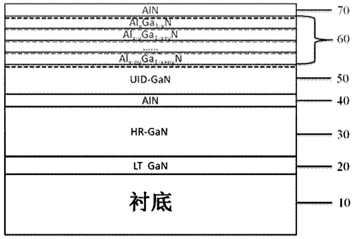
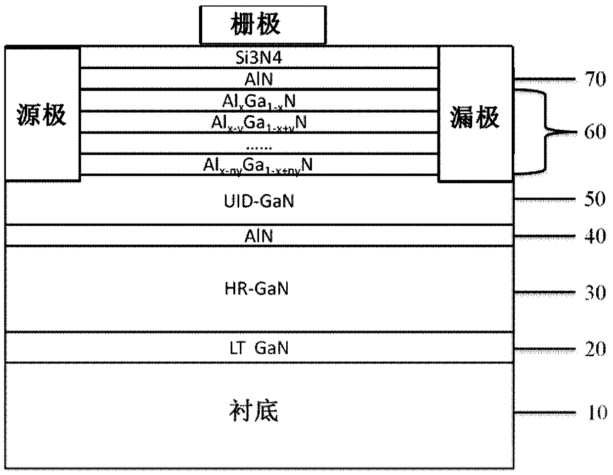
[0030] Step 1: growing a low-temperature GaN buffer layer on the substrate;
[0031] Step 2: growing an undoped high-resistance GaN layer on the low-temperature GaN buffer layer;
[0032] Step 3: growing an AlN isolation layer on the undoped high-resistance GaN layer;
[0033] Step 4: growing an undoped GaN channel layer on the AlN isolation layer;
[0034] After step 4, a barrier layer with stepwise change in Al composition is grown on the undoped GaN channel layer, and an AlN barrier layer is grown on the barrier layer with stepwise change in Al composition, thereby generating a multi-channel structure.
Login to View More PUM
| Property | Measurement | Unit |
|---|---|---|
| thickness | aaaaa | aaaaa |
| thickness | aaaaa | aaaaa |
Abstract
The invention discloses an HEMT epitaxial structure, which structurally comprises a substrate (10), a low-temperature GaN buffer layer (20), an undoped GaN high-resistance layer (30), an AlN isolation layer (40), an undoped GaN channel layer (50), a barrier layer (60) with the Al content thereof to be changing in the stepped manner, and an AlN barrier layer (70). The undoped GaN high-resistance layer and the AlN isolation layer grow after the annealing treatment of the low-temperature GaN buffer layer. Compared with the carbon-doped manner or the iron-doped manner, the crystallization quality is effectively improved and the memory effect caused by ion doping is avoided. Meanwhile, the structure is provided with multiple channels, wherein two main channels are formed at the interfaces of an AlN barrier layer and an undoped GaN channel layer with the barrier layer with the Al content thereof to be changing in the stepped manner, and multiple auxiliary channels are formed at the interface of the barrier layer with the Al content thereof to be changing in the stepped manner. Compared with a conventional HEMT device, the current driving capability of the HEMT device is enhanced. The gate leakage current of the HEMT epitaxial structure and the leakage current of the buffer layer are small, and the current driving capability is strong. Therefore, the HEMT epitaxial structure can be applied to the field of high-power electronic devices. In addition, the invention further provides a preparation method of the HEMT epitaxial structure.
Description
technical field [0001] The invention belongs to the field of power electronic device materials, and in particular relates to HEMT epitaxy technology. Background technique [0002] Currently, the main methods for growing a high-resistance buffer layer for HEMT devices include introducing C impurities and introducing Fe impurities. However, the complexity of the process is increased by doping and the crystal quality of the crystal is deteriorated; Luo W et al. [Journal of Alloys & Compounds 633 (2015): 494-498] made the resistance reach 10 by changing the annealing atmosphere 8 ohm / sq, but this value does not meet the requirements of HEMT HR-GaN. Therefore, it is necessary to explore a simpler and more effective method for growing a high-resistance buffer layer. [0003] In addition, common HEMT epitaxy is single-channel conductive, which limits the improvement of output power. Existing multi-channel HEMTs often introduce InGaN barrier layers or carry out n-type doping, etc...
Claims
Login to View More Application Information
Patent Timeline
 Patent Type & AuthorityPatents(China)
IPC IPC(8): H01L29/778H01L21/335
Inventor吉泽生汪连山赵桂娟孟钰淋李辉杰谭晓宇韩东岳杨少延王占国
OwnerINST OF SEMICONDUCTORS - CHINESE ACAD OF SCI