

Polycrystalline silicon ingot casting technology
A polycrystalline silicon ingot furnace and polycrystalline silicon technology are applied in the directions of polycrystalline material growth, crystal growth, single crystal growth, etc., which can solve the problems of difficulty in removing crucible gas, high oxygen content in ingot products, poor use effect, etc. The effect of grain size, low input cost and easy control
- Summary
- Abstract
- Description
- Claims
- Application Information
AI Technical Summary
Problems solved by technology
Method used
Image

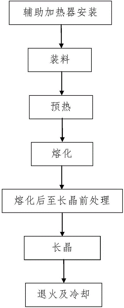
Examples
Embodiment 2
[0216] In this example, the difference from Example 1 is that in step 101, the organic binder, deionized water and boron nitride are uniformly mixed at a mass ratio of 1:2:0.8 to obtain a coating spray solution; the organic binder The agent is a silicone adhesive; when spraying in step 102, the inner bottom surface of the crucible 1 is 1m 2 The mass of boron nitride contained in the coating spray liquid sprayed in the area is 100g; when drying in step 103, the drying equipment is used to spray on the inner bottom surface of the crucible 1 at a temperature of 80°C The coating spray liquid is dried, and the crucible 1 is heated to 80° C. by the drying equipment, and then kept warm until the coating spray liquid sprayed on the inner bottom surface of the crucible 1 is dried; the steps The preheating time in the third step is 4h and T1=1285°C, P1=100kW; T2=1400°C in step 401, T3=1560°C in step 402, t=20min in step 403, P2=45kW; Q2=650mbar in step 4 ; In the first step, the holdin...
Embodiment 3
[0227] In this example, the difference from Example 1 is that in step 101, the organic binder, deionized water and boron nitride are uniformly mixed in a mass ratio of 1:2.5:0.8 to obtain a coating spray solution; the organic binder The agent is an epoxy adhesive; when spraying in step 102, the inner bottom surface of the crucible 1 is 1m 2 The mass of boron nitride contained in the coating spray liquid sprayed in the area is 130g; when drying in step 103, the drying equipment is used to spray on the inner bottom surface of the crucible 1 at a temperature of 100°C Dry the coating spray liquid, and first use the drying equipment to heat the crucible 1 to 100°C, and then keep it warm until the coating spray liquid sprayed on the inner bottom surface of the crucible 1 is dried; step The preheating time in the third step is 6h and T1=1125°C, P1=50kW; T2=1350°C in step 401, T3=1540°C in step 402, t=40min in step 403, P2=25kW; Q2=550mbar in step 4 ; In the first step, the holding t...
Embodiment 4
[0238] In this example, the difference from Example 1 is that in step 101, the organic binder, deionized water and boron nitride are uniformly mixed at a mass ratio of 1:2.5:1.2 to obtain a coating spray solution; the organic binder The agent is an instant adhesive; when spraying in step 102, the inner bottom surface of the crucible 1 is 1m 2 The mass of boron nitride contained in the coating spray liquid sprayed in the region is 180g.
[0239] In this embodiment, the remaining method steps and process parameters are the same as those in Embodiment 1.
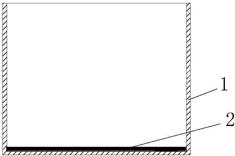
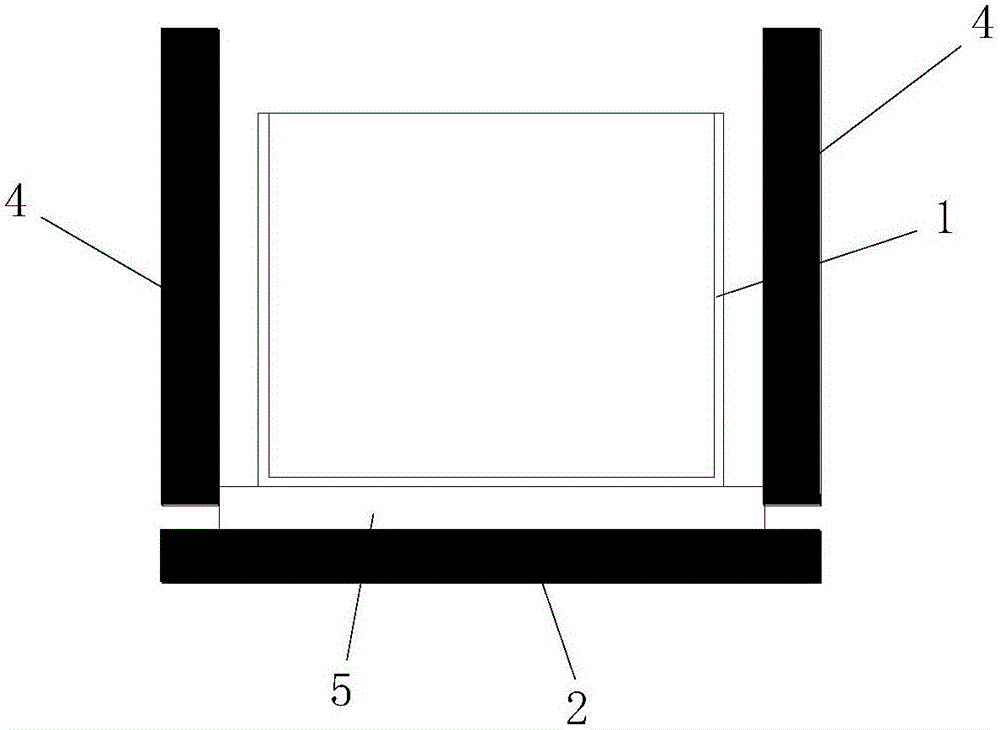
[0240] In this embodiment, compared with the conventional crucible, after the polysilicon ingot casting furnace is used and the crucible 1 with the bottom coating 2 is used for polysilicon ingot casting, the surface of the processed ingot finished product has no impurities, no sticking crucible phenomenon, and the bottom of the ingot is The oxygen content is reduced by more than 72%, the minority carrier lifetime is more than ...
PUM
| Property | Measurement | Unit |
|---|---|---|
| mass | aaaaa | aaaaa |
| mass | aaaaa | aaaaa |
Abstract
Description
Claims
Application Information