Method for preparing force response photonic crystal material on basis of nano molding technique

A nano-molding technology and photonic crystal technology, applied in the field of preparation of photonic crystal materials, can solve the problems of difficulty in preparing nano-scale photonic crystals, limited precision of photonic crystals, poor structural controllability, etc. The effect of short preparation cycle and reduced preparation cost

Active Publication Date: 2017-01-04
SHANDONG UNIV OF SCI & TECH
View PDF5 Cites 9 Cited by
  • Summary
  • Abstract
  • Description
  • Claims
  • Application Information

AI Technical Summary

Problems solved by technology

Therefore, it is difficult to prepare nanoscale photonic crystals by laser holographic interferometry
[0007] In a nutshell, the existing photonic crystal material preparation methods generally have the follow

Method used


Image

  • Method for preparing force response photonic crystal material on basis of nano molding technique
  • Method for preparing force response photonic crystal material on basis of nano molding technique
  • Method for preparing force response photonic crystal material on basis of nano molding technique

Examples


Example Embodiment

[0048] Example 1

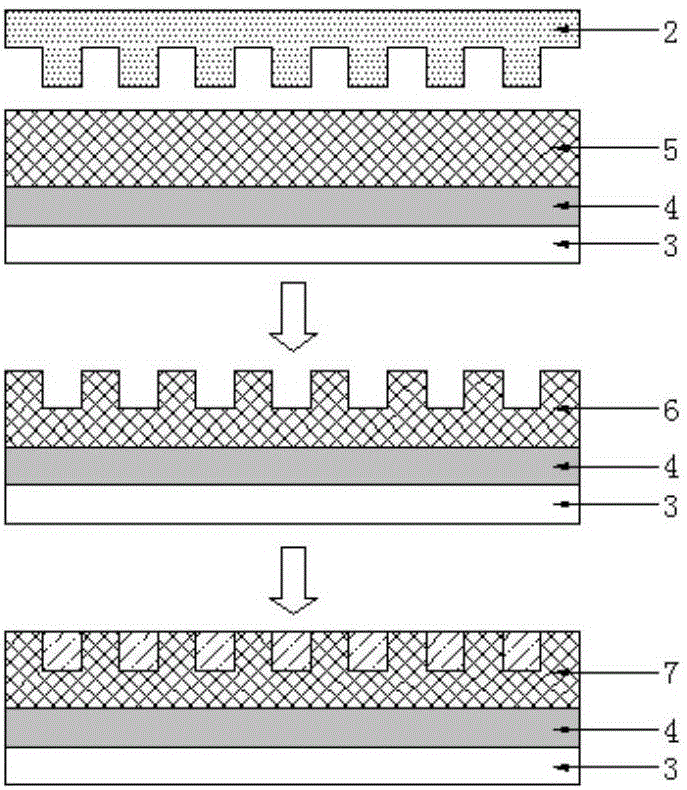
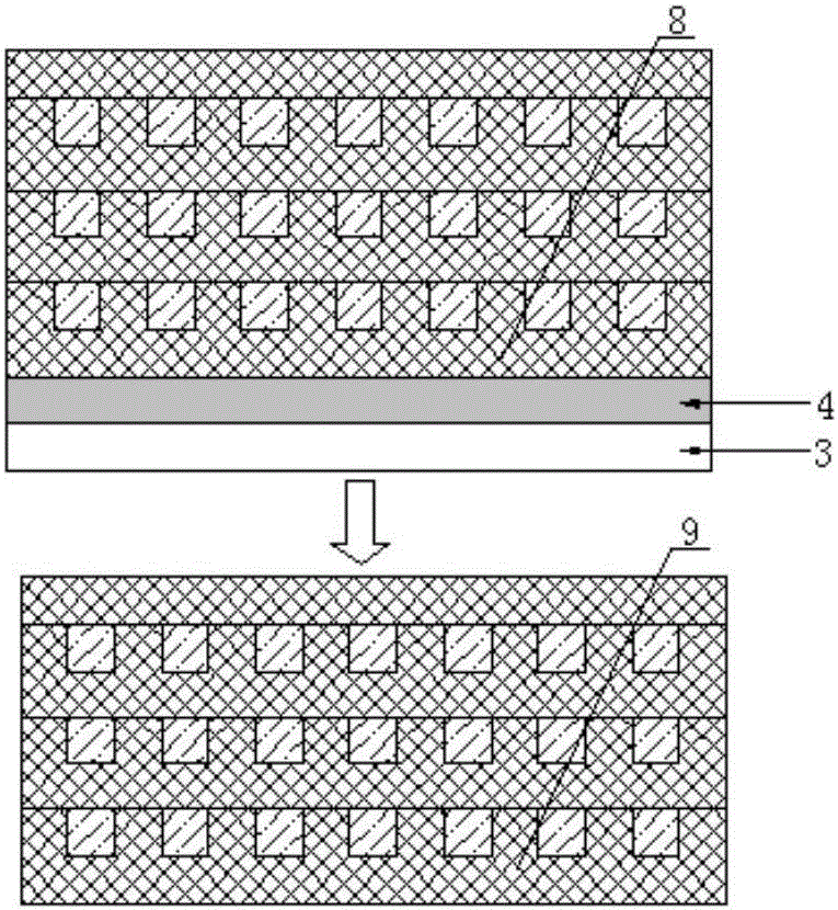
[0049] The preparation method of the force-responsive photonic crystal material is as follows:

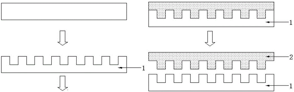
[0050] 1. If figure 1 As shown, the preparation steps of the quartz master template are as follows:

[0051] (1) Pre-design the structural parameters of the photonic crystal according to the actual needs, mainly including: the surface structure is a hexagonally arranged columnar lattice, the lattice period is 200nm, the diameter of the raised column is 100nm, and the height of the raised column is 150nm, The effective area is 20×20mm 2 .

[0052] (2) Take a quartz substrate (size is 25mm×25mm), according to the structural parameters of the above-mentioned photonic crystal, use electron beam lithography to expose the quartz substrate and the photoresist on it for 30s, and obtain a band after developing. There is a photoresist with a design pattern; then, the quartz substrate and the photoresist on it are etched for 20 minutes by reactive ion etching technology...


PUM


Abstract

The invention discloses a method for preparing a force response photonic crystal material on the basis of a nano molding technique. The method comprises the following steps: etching a main template according to pre-designed photonic crystal structure parameters, preparing an elastic polymer soft template with inverse nano-grade patterns, and by taking the soft template as a secondary template, 'copying' the patterns on the main template into a high -elasticity gel matrix layer in a 'high-fidelity 'manner in a mode of three-step pattern transfer so as to fix the position of crystal lattice of photonic crystal; filling the crystal lattice with a viscous polymer so as to obtain a single-layer high-elasticity gel-viscous polymer composite layer with a photonic crystal structure, and implementing a layer-by -layer embossing method,thereby obtaining the force response photonic crystal material. Compared with the prior art,the method disclosed by the invention has the characteristics that the process is simple, the procedure time is short, process parameters are easy to control, the templates can be repeatedly used, and a product is high in precision grade, stable and reliable in quality and relatively low in cost, and the like.

Description

technical field [0001] The invention relates to a method for preparing a photonic crystal material, in particular to a method for preparing a force-responsive photonic crystal material based on nano-molding technology. Background technique [0002] The preparation of the force-responsive photonic crystal material is completed by filling the highly elastic gel material with excellent mechanical properties in the nanoscale photonic crystal lattice gap. Through mechanical stretching or compression, the highly elastic polymeric network structure will increase or decrease the lattice spacing of photonic crystals, resulting in changes in diffraction wavelength and structural color, and realize the transformation of physical deformation into optical performance changes. Sensing function. Studies have shown that the multilayer structure composed of highly elastic gel and viscoelastic polymer with nanoscale photonic crystal structure has good mechanical response performance. This k...

Claims


Application Information

Patent Timeline
IPC IPC(8): G02B1/00
CPCG02B1/005
Inventor 王清张睿郑旭马立俊张艳菊张星远杜文全
Owner SHANDONG UNIV OF SCI & TECH
Why Eureka
Try Eureka