Supercharge Your Innovation With Domain-Expert AI Agents!

Method for thinning grid oxide layer and method for manufacturing MOS device

A technology of gate oxide layer and manufacturing method, which is applied in semiconductor/solid-state device manufacturing, semiconductor devices, electrical components, etc., to achieve the effects of avoiding lateral etching, uniform thickness of gate oxide layer, and avoiding lateral damage

Inactive Publication Date: 2017-01-04
SEMICON MFG INT (SHANGHAI) CORP
View PDF4 Cites 4 Cited by
  • Summary
  • Abstract
  • Description
  • Claims
  • Application Information

AI Technical Summary

Problems solved by technology

[0008] In order to solve the problems existing in the gate etching method of the existing semiconductor device, the application provides a method for thinning the gate oxide layer and a manufacturing method of the MOS device

Method used


Image

  • Method for thinning grid oxide layer and method for manufacturing MOS device
  • Method for thinning grid oxide layer and method for manufacturing MOS device
  • Method for thinning grid oxide layer and method for manufacturing MOS device

Examples


Embodiment 1

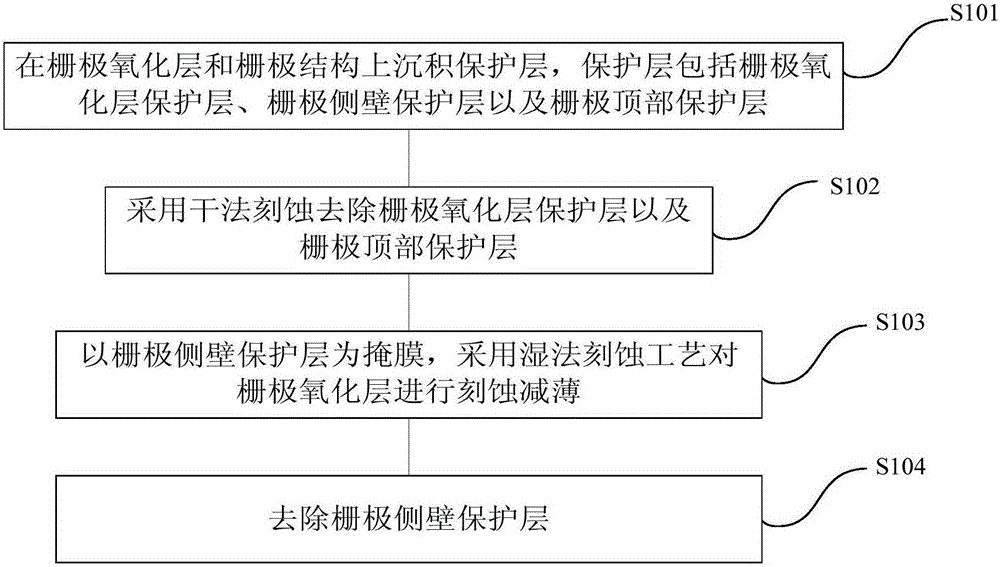
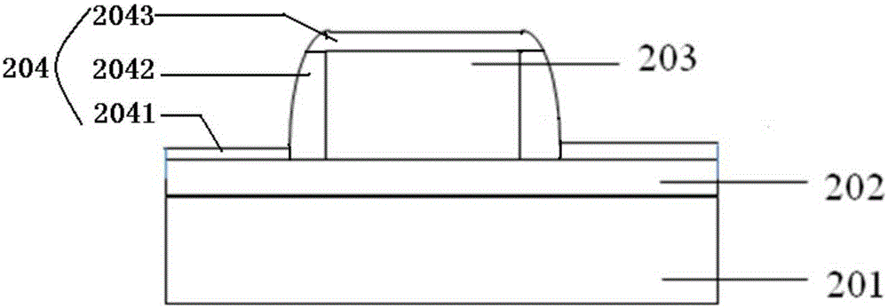
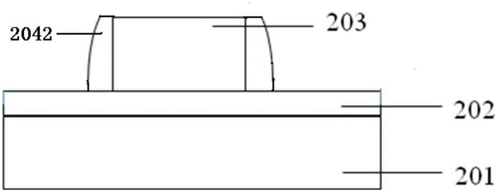
[0042] Provide a P-type silicon substrate, deposit a silicon dioxide layer (gate oxide layer) with a thickness of 10 nanometers on the P-type silicon substrate, and then form a source on the silicon wafer through photolithography, etching and electrode material deposition processes Electrode, drain, gate; Deposit a silicon nitride film (protective layer) on the surface of the gate and silicon dioxide layer by chemical vapor deposition process, the thickness of the silicon nitride film is 30 nanometers; remove by dry etching The silicon nitride film on the top of the gate and the surface of the gate oxide layer, the silicon nitride film on the side wall of the gate is retained, the etching gas is oxygen and fluorine-containing gas, the reaction power is 300 watts, and the etching temperature is 50 ° C. The etching time is 15 seconds; immerse the wafer in the HF etching solution, let the HF etching solution react with the gate oxide layer on the substrate for 500 seconds, then gr...

Embodiment 2

[0047] Provide a P-type silicon substrate, deposit a silicon dioxide layer with a thickness of 20 nanometers on the silicon wafer, and then form the source and drain electrodes on the silicon wafer through photolithography, etching and electrode material deposition processes; through chemical vapor deposition The process deposits a silicon nitride film on the surface of the gate and the oxide layer as a gate protection layer, and the thickness of the titanium nitride film is 45 nanometers; the protection on the top of the gate and the surface of the gate oxide layer is removed by dry etching layer, the etching gas is oxygen and helium, the sputtering power is 300 watts, the etching temperature is 50°C, and the etching time is 12 seconds; the wafer is immersed in the HF etching solution, and the HF etching solution and the substrate The oxide layer on the bottom reacts for 500 seconds, and then the gate oxide layer is gradually peeled off. The stripped product leaves the etched ...


PUM

PropertyMeasurementUnit
Thicknessaaaaaaaaaa
Thicknessaaaaaaaaaa
Thicknessaaaaaaaaaa

Abstract

The invention provides a method for thinning a grid oxide layer and a method for manufacturing an MOS device. The method comprises the steps of (S101) depositing a protection layer on a gate oxide layer and a gate structure, wherein the protection layer comprises a gate oxide layer protection layer, a gate side wall protection layer and a gate top protection layer, (S102) using a dry etching method to remove the gate oxide layer protection layer and the gate top protection layer, (S103) with the gate side wall protection layer as a mask, using a wet etching process to carry out etching thinning on the gate oxide layer, and (S104) removing the above gate side wall protection layer. The thickness of the gate oxide layer of a semiconductor device obtained by etching according to the above method is uniform, and the technical defects brought by existing etching process are overcome.

Description

technical field [0001] The present application relates to a manufacturing process of a semiconductor integrated circuit, in particular to a method for thinning a gate oxide layer and a manufacturing method of a MOS device. Background technique [0002] At present, with the rapid development of semiconductor manufacturing technology, in order to achieve faster computing speed, larger data storage capacity and more functions of semiconductor devices, chips are developing towards the direction of high component density and high integration. Among them, gates of semiconductor devices are becoming thinner and shorter than before, and oxide layers of gates are becoming thinner and thinner. [0003] In semiconductor products, both high-voltage devices and low-voltage devices are usually involved. In general, the thickness of the gate oxide layer in high-voltage devices is larger than that in low-voltage devices. Therefore, in the production process, it is necessary to etch and th...

Claims


Application Information

Patent Timeline
IPC IPC(8): H01L21/311H01L21/32H01L21/336
CPCH01L21/31111H01L21/31116H01L21/31144H01L29/66477
Inventor 赵连国彭坤
Owner SEMICON MFG INT (SHANGHAI) CORP
Features
  • R&D
  • Intellectual Property
  • Life Sciences
  • Materials
  • Tech Scout
  • Unparalleled Data Quality
  • Higher Quality Content
  • 60% Fewer Hallucinations
Learn More