VDMOS device and manufacturing method therefor

A manufacturing method and device technology, applied in semiconductor/solid-state device manufacturing, semiconductor devices, electrical components, etc., can solve problems such as lower device yield, short circuit of metal layer and polysilicon layer, etc., to avoid connectivity and improve output The effect of yield

Active Publication Date: 2017-01-04
FOUNDER MICROELECTRONICS INT
View PDF4 Cites 2 Cited by
  • Summary
  • Abstract
  • Description
  • Claims
  • Application Information

AI Technical Summary

Problems solved by technology

[0005] The invention provides a method for manufacturing a VDMOS device, so as to overcome the technical problem that the short circuit between the metal layer and the polysilicon layer in the subsequent process caused by the offset of the contact hole in the prior art leads to a decrease in the yield of the device.

Method used


Image

  • VDMOS device and manufacturing method therefor
  • VDMOS device and manufacturing method therefor
  • VDMOS device and manufacturing method therefor

Examples


Embodiment 1

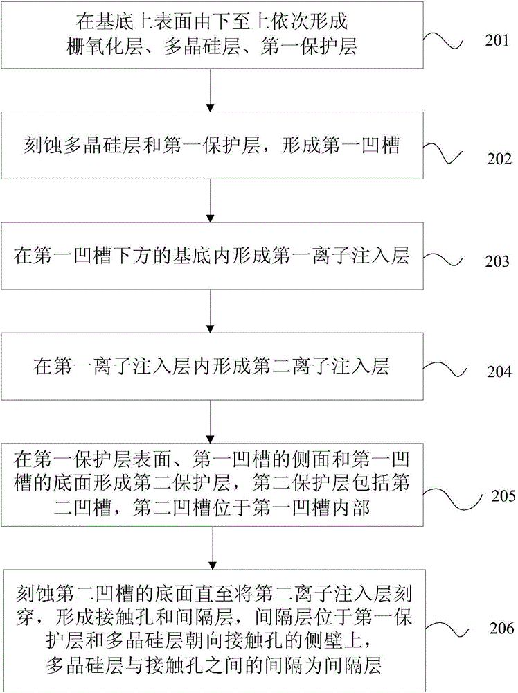
[0013] This embodiment provides a method for manufacturing a VDMOS device. figure 2 It is a flow chart of the manufacturing method of the VDMOS device of the present embodiment, as figure 2 As shown, the VDMOS device manufacturing method may include:

[0014] In step 201, a gate oxide layer, a polysilicon layer, and a first protective layer are sequentially formed on the upper surface of the substrate from bottom to top.

[0015] Specifically, firstly, a gate oxide layer is formed on the upper surface of the substrate by chemical vapor deposition, and the growth temperature is 900°C-1100°C. Of course, the gate oxide layer can also be formed by oxidizing the substrate. The oxidation time can vary with the specific formation of the gate oxide layer. to change the thickness. Further, a polysilicon layer is chemically vapor deposited on the gate oxide layer at a growth temperature of 500°C-700°C, and the first protective layer is formed by oxidizing the surface of the polysili...

Embodiment 2

[0028] In order to better describe the first embodiment, this embodiment is based on the above-mentioned embodiment and adds drawings to explain the above-mentioned embodiment. Such as Figures 3A to 3G Show, Figures 3A-3G It is a structural schematic diagram of each step of making a VDMOS device.

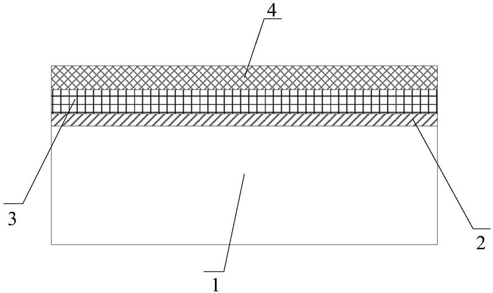
[0029] Such as Figure 3A As shown, a gate oxide layer 2 , a polysilicon layer 3 , and a first protection layer 4 are sequentially formed on the upper surface of the substrate 1 from bottom to top. Specifically, the base 1 includes a substrate and an epitaxial layer, and the thickness of the polysilicon layer 3 is 0.2 micron-1.0 micron. Wherein, the thickness of the first protection layer 4 is greater than the thickness of the gate oxide layer 2 .

[0030] Such as Figure 3B As shown, the polysilicon layer 3 and the first protective layer 4 are etched to form the first groove 5 .

[0031] Wherein, the first protection layer 4 is to protect the polysilicon layer 3 and prevent...

Embodiment 3

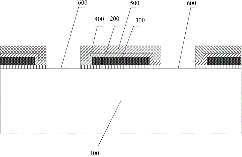
[0040] This embodiment provides a VDMOS device, and the VDMOS device can be manufactured according to the manufacturing method of the VDMOS device in the foregoing embodiments. Among them, such as Figure 3G As shown, the VDMOS device includes: a substrate 1, and a gate oxide layer 2, a polysilicon layer 3, a first protective layer 4, a contact hole 9, a spacer layer 810, and a first ion implantation layer formed sequentially on the upper surface of the substrate 1 from bottom to top. Layer 6, the second ion implantation layer 7.

[0041] Wherein, the contact hole 9 is formed in the gate oxide layer 2 , the polysilicon layer 3 and the first protection layer 4 , and the bottom of the contact hole 9 is located in the substrate 1 . The contact hole 9 penetrates through the gate oxide layer 2 , the polysilicon layer 3 and the first protection layer 4 . Specifically, firstly, the gate oxide layer 2 is formed on the upper surface of the substrate 1 by chemical vapor deposition, an...


PUM

PropertyMeasurementUnit
thicknessaaaaaaaaaa
thicknessaaaaaaaaaa
thicknessaaaaaaaaaa

Abstract

The invention discloses a VDMOS device and a manufacturing method therefor. The manufacturing method comprises the steps of forming a gate oxide layer, a polysilicon layer and a first protection layer on the upper surface of a substrate from the bottom up in sequence; etching the polysilicon layer and the first protection layer to form first grooves; forming a first ion implantation layer in the substrate below the first grooves; forming a second ion implantation layer in the first ion implantation layer; forming a second protection layer on the surface of the first protection layer, the side surfaces and the bottom surfaces of the first grooves, wherein the second protection layer comprises second grooves which are formed in the corresponding first grooves; and etching the bottom surfaces of the second grooves until the second ion implantation layer is thoroughly etched to form contact holes and an interval layer. According to the VDMOS device and the manufacturing method therefor, the contact holes are formed by adopting a self-alignment way, so that offset of the contact holes is avoided, namely, the connection between the contact holes and the polysilicon layer is avoided, thereby improving the output yield of the device.

Description

technical field [0001] The invention relates to a semiconductor device and a manufacturing method thereof, in particular to a VDMOS device and a manufacturing method thereof. Background technique [0002] Vertical double-diffused metal oxide semiconductor devices (VDMOS, vertical double-diffused Metal Oxide Semiconductor) are widely used in switching power supplies, automotive electronics due to their high input impedance, low drive power, and superior frequency characteristics and thermal stability. , Motor drives, high frequency oscillators and many other fields. [0003] figure 1 It is a schematic structural diagram of a VDMOS device in the prior art (patterns with the same texture represent the same layer), and the VDMOS device includes: a substrate 100, a gate oxide layer 200, a polysilicon layer 300, a silicon nitride layer 400, a dielectric layer 500, and a contact hole 600 , wherein the contact hole 600 is formed by photolithography. [0004] However, due to the d...

Claims


Application Information

Patent Timeline
Patent Type & Authority Applications(China)
IPC IPC(8): H01L29/78H01L21/768
Inventor 马万里任春红
Owner FOUNDER MICROELECTRONICS INT
Why Eureka
Try Eureka