Five-junction solar cell based on inp substrate and preparation method thereof

A solar cell and substrate technology, applied in the field of solar photovoltaics, can solve the problems that affect the performance of the fourth sub-cell of InGaP, the overall performance of the four-junction cell, the inability to achieve current matching, and reduce the performance of the cell, so as to improve the conversion efficiency of the cell and divide it meticulously , the effect of reducing production costs

Active Publication Date: 2017-10-24
苏州镓港半导体有限公司
View PDF1 Cites 3 Cited by
  • Summary
  • Abstract
  • Description
  • Claims
  • Application Information

AI Technical Summary

Problems solved by technology

The energy band width of the four-junction cell structure is not the most ideal combination, the bandwidth of the third sub-cell is too small, it is easy to generate too much current and cannot achieve current matching, which reduces the performance of the cell; a

Method used


Image

  • Five-junction solar cell based on inp substrate and preparation method thereof
  • Five-junction solar cell based on inp substrate and preparation method thereof
  • Five-junction solar cell based on inp substrate and preparation method thereof

Examples


Embodiment 1

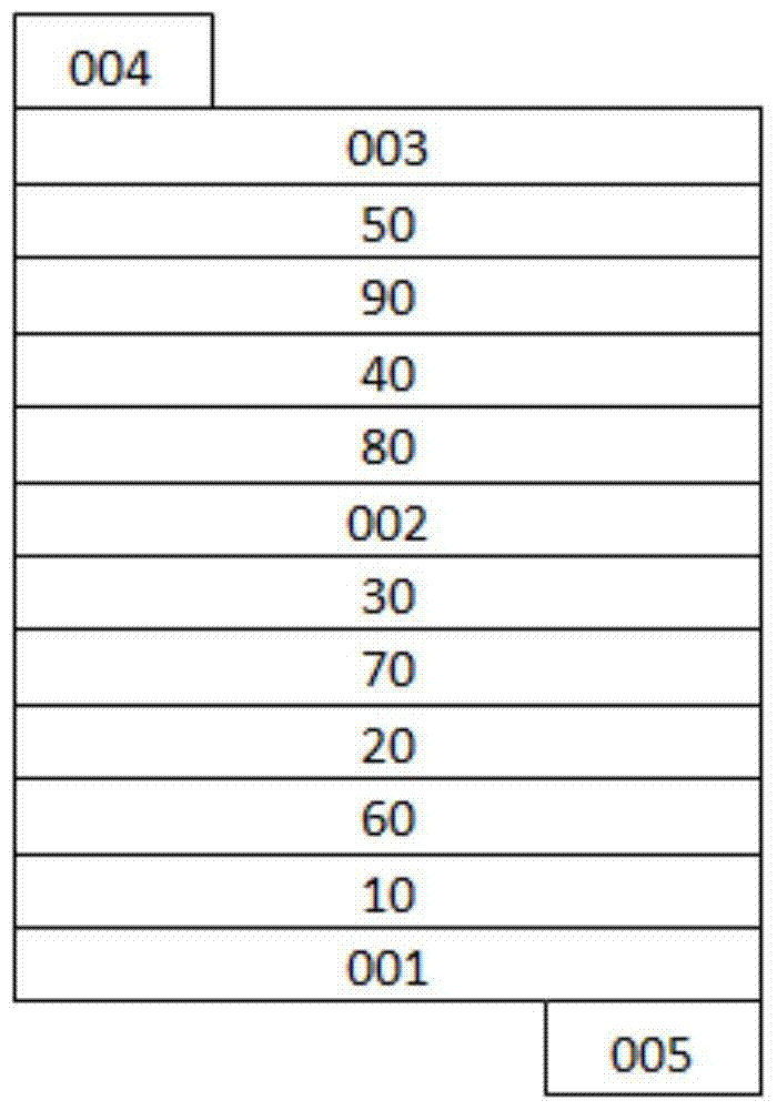
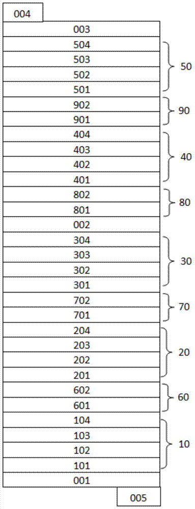
[0049] Use MOCVD (Metal Organic Chemical Vapor Deposition) as the growth process to provide p-type InP substrate 001, and the growth source is TMGa, TMAl, TMIn, AsH 3 and PH 3 , the dopant source n-type is Si 2 h 6 , p-type is DEZn and CBr 4 . The growth temperature is about 650°C, and the reaction chamber pressure is 100 Torr. After high temperature treatment to remove impurities on the surface of the substrate, according to image 3 The five-junction solar cell structure shown grows each layer structure sequentially.

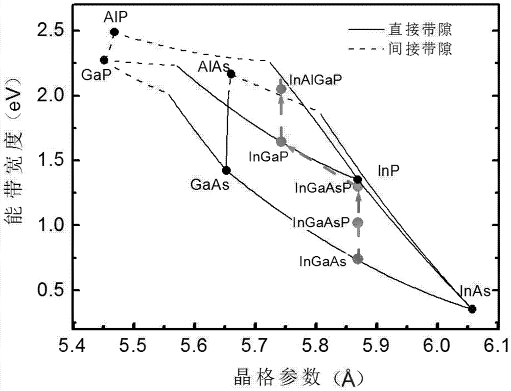
[0050] (1), InGaAsP first subcell 10: p-type InP (1×10) doped with Zn comprising 0.2 microns thick 18 cm -3 ) the first back field layer 101, 2.5 micron thick p-type InGaAsP doped with Zn (2×10 17 cm -3 ) n-type InGaAsP doped with Si (2×10 18 cm -3 ) the first emitter region 103 and 0.05 micron thick n-type InAlGaAs doped with Si (5×10 18 cm -3 ) first window layer 104. Wherein, the p-type InGaAsP first base region 102 and the n-type InGaAsP firs...

Embodiment 2

[0064] Use MOCVD as the growth method, provide p-type InP substrate 001, and the growth source is TMGa, TMAl, TMIn, AsH 3 and PH 3 , the dopant source n-type is Si 2 h 6 and DETe, p-type is DEZn and CBr 4 . The growth temperature is about 650°C, and the reaction chamber pressure is 100 Torr. After high temperature treatment to remove impurities on the surface of the substrate, according to image 3 The five-junction solar cell structure shown grows each layer structure sequentially.

[0065] (1), InGaAsP first subcell 10: p-type InP (1×10) doped with Zn comprising 0.2 microns thick 18 cm -3 ) the first back field layer 101, 2.5 micron thick p-type InGaAsP doped with Zn (2×10 17 cm -3 ) n-type InGaAsP doped with Si (2×10 18 cm -3 ) first emitter region 103 and 0.05 micron thick n-type InP doped with Si (5×10 18 cm -3 ) first window layer 104. Wherein, the p-type InGaAsP first base region 102 and the n-type InGaAsP first emitter region 103 are lattice-matched with ...

Embodiment 3

[0079] Using MBE (molecular beam epitaxy) as the growth process, a p-type InP substrate 001 is provided, the growth source is solid single source Ga, Al, In, As and P, the n-type dopant source is Si, and the p-type is Be and C. The growth temperature is about 500°C. After the substrate is degassed and impurity removed, according to the following image 3 The five-junction solar cell structure shown grows each layer structure sequentially.

[0080] (1), InGaAsP first subcell 10: p-type InP (1×10 18 cm -3 ) the first back field layer 101, 2.5 micron thick p-type InGaAsP (2×10 17 cm -3 ) n-type InGaAsP doped with Si (2×10 18 cm -3 ) the first emitter region 103 and 0.05 micron thick n-type InAlGaAs doped with Si (5×10 18 cm -3 ) first window layer 104. Wherein, the p-type InGaAsP first base region 102 and the n-type InGaAsP first emitter region 103 are lattice-matched with the InP substrate 001, the bandwidth is 0.78eV, and the corresponding P composition is 8%.

[0081...


PUM


Abstract

The invention discloses a five-junction solar cell based on an InP substrate, which comprises the InP substrate, and an InGaAsP first sub cell, a first tunnel junction, an InGaAsP second sub cell, a second tunnel junction, an InGaAsP third sub cell, a gradient buffer layer, a third tunnel junction, an InGaP fourth sub cell, a fourth tunnel junction, an InAlGaP fifth sub cell and an InGaAs contact layer sequentially arranged on the InP substrate. The invention also discloses a method of preparing the above five-junction solar cell. The former three junctions of sub cells of the five-junction solar cell provided by the invention are in lattice match with the InP substrate, the latter two junctions of In(Al)GaP sub cells have mutant lattices. Current match among sub cells is realized through reasonable bandwidth selection, and a high photoelectric conversion efficiency is achieved.

Description

technical field [0001] The invention relates to the field of solar photovoltaic technology, in particular to a five-junction solar cell based on an InP substrate and a preparation method thereof. Background technique [0002] Group V / III multi-junction solar cells can divide the solar spectrum into multiple energy segments and absorb them separately. The conversion efficiency is the highest among all solar cell technologies. Currently, the most mature technology is based on lattice-matched InGaP / GaAs / Ge triple-junction cells. The average conversion efficiency of its large-scale production is about 40%. However, in the InGaP / GaAs / Ge triple-junction cell, because the Ge sub-cell at the bottom junction produces almost twice the current of the InGaP and GaAs sub-cells, it is not the best energy band combination. Many companies and scientific research institutions are working on how to In order to achieve current matching and improve battery efficiency, research and development ...

Claims


Application Information

Patent Timeline
IPC IPC(8): H01L31/0725H01L31/0328
CPCY02E10/50
Inventor 黄勇
Owner 苏州镓港半导体有限公司
Why Eureka
Try Eureka